A
B
C
D
Text Solution
Verified by Experts


TARGET PUBLICATION-SEMICONDUCTORS-EXERCISE
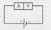
- in the foll. Circuit of PN junction , diodes D1, D2 and D3 are ideal t...
Text Solution
|
- OF THE DIODES SHOWN IN the foll. Diagrams, which one is reverse biased...
Text Solution
|
- a semiconductorX is made by doping a germanium crytsal with arsenic (z...
Text Solution
|
- the dominant mecahnisms for motion of chargecarriers in forward and re...
Text Solution
|
- serious draback of the semiconductors devices is
Text Solution
|
- in LED, to avoid damage to the diode is used
Text Solution
|
- in LED, intensity of emitted light
Text Solution
|
- which of the foll. Is NOT an appliction of photodiode?
Text Solution
|
- in a p-n junction photo cell, the value of photo-electromotive force p...
Text Solution
|
- Assertion :light emitting diode (LED) emits spontaneous radiation reas...
Text Solution
|
- thermistors may have
Text Solution
|
- which of the foll. Graphs represents NTC thermistors
Text Solution
|
- the circuit has two oppositely connected ideal diodes in parallel. Wha...
Text Solution
|
- a p-n junction diode when forward biased has a drop of 0.4 V which is ...
Text Solution
|
- for a photodiode , the forbidden energy gap (E8)of the material used i...
Text Solution
|
- if the band gap between valence band and conduction band in a matereia...
Text Solution
|
- in insulatore (C.B. is conduction band and V.B. is a valence band)
Text Solution
|
- the energy gap in case of which of the foll. Is less than 3eV?
Text Solution
|
- the band gap of an insulator , conductor and semic conductor are E(gI)...
Text Solution
|
- C and Si bot have same lattice structure , having bomnding electrons ...
Text Solution
|