A
B
C
D
Text Solution
Verified by Experts


Topper's Solved these Questions
Similar Questions
Explore conceptually related problems
TARGET PUBLICATION-SEMICONDUCTORS-EXERCISE
- The given graph represents V-I characteristics for a semiconductor dev...
Text Solution
|
- A wire of aluminum and a wire of germanium are cooled to a temperature...
Text Solution
|
- which of the foll. Statement is not true?
Text Solution
|
- In Gallium Arsenide material, Ohm's law does not hold good because
Text Solution
|
- An LED is constructed from a p-n junction based on a certain semi cond...
Text Solution
|
- Generally, the no. of electrons in the valence shell of good conductor...
Text Solution
|
- the process of addding impurities to the pure semiconductor is called
Text Solution
|
- the intrinsic semiconductors becomes an insulator at
Text Solution
|
- a p -type semiconductor is (i) a silicon crystal doped with arsenic im...
Text Solution
|
- when forward bias is appllied to as p-n junction . Then wat happens to...
Text Solution
|
- a Ge specimen is doped with AI the concentartion of acceptor atoms is ...
Text Solution
|
- if the two ends p and n of p-n junction diode are joined by a wire,
Text Solution
|
- a light emitted diode is
Text Solution
|
- in remote controlled receivers , the sensors are
Text Solution
|
- the temoperature -coefficient of resistivity of semiconductors is
Text Solution
|
- carbon , silicon and germanium have four valence electrions each . The...
Text Solution
|
- the no. densities of electrons and holes in a pure germanium at room t...
Text Solution
|
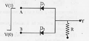
- the circuit below represents a
Text Solution
|
- The maximum wavelength which a photodiode can detect with Eg =0.74eV i...
Text Solution
|
- When p-n junction is reverse biased, then the width of barriers potent...
Text Solution
|