Text Solution
Verified by Experts


Similar Questions
Explore conceptually related problems
Recommended Questions
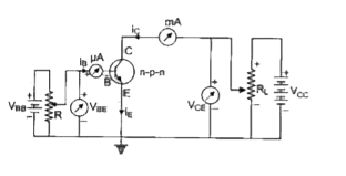
- (i) Draw a circuit diagram to study the input and output characteristi...
Text Solution
|
- With the help of a labelled circuit diagram, explain how an n-p-n tran...
Text Solution
|
- In a common emitter amplifier circuit using an n-p-n transistor, the p...
Text Solution
|
- n - p - n ट्रांजिस्टर के उभयनिष्ठ-उत्सर्जक प्रवर्धन की क्रिया, परिपथ ...
Text Solution
|
- n - p - n ट्रांजिस्टर से बनाये हुए एक उभयनिष्ठ-उत्सर्जक प्रवर्धक परिपथ...
Text Solution
|
- Draw the circuit diagram for studying the characteristics of a transis...
Text Solution
|
- उभयनिष्ठ उत्सर्जक N - P - N ट्रांजिस्टर प्रवर्धक का परिपथ चित्र बनाइए...
Text Solution
|
- In a common-emitter amplifier circuit using an n-p-n transistor the ph...
Text Solution
|
- Draw the circuit diagram for studying the characteristics of a transis...
Text Solution
|