


Topper's Solved these Questions
Similar Questions
Explore conceptually related problems
R G PUBLICATION-ELECTRONIC DEVICES-EXERCISE
- Give a comparative discussion on majority and minority carriers in n-t...
Text Solution
|
- Draw a circuit diagram of a full rectifier and explain its working.
Text Solution
|
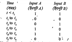
- Sketch inputs A,B and output Y from a NAND gate from the table given b...
Text Solution
|
- Explain, how a transistor can be used as a switch with the help of a c...
Text Solution
|
- For a Common emitter emplifer the output voltage across collector resi...
Text Solution
|
- How can you realise an OR gate using three NAND gates? Explain with ci...
Text Solution
|
- In the aboe circuit diagram Vcc=8V, Vout=0.5V, RL=800Omega and alpha=0...
Text Solution
|
- Draw diagrams to show how a p-n junction is forward biased Draw V-I ...
Text Solution
|
- Draw diagrams to show how a p-n junction is forward biased Draw V-I ...
Text Solution
|
- Draw a circuit diagram of a transistor amplifier in CE configuration. ...
Text Solution
|
- Draw a circuit diagram of a transistor amplifier in CE configuration. ...
Text Solution
|
- Difference between intrinsic and extrinsic semiconductor?
Text Solution
|
- What is doping?
Text Solution
|
- What is intrinsic carrier concentration?
Text Solution
|
- C,Si and Ge have the same lattice structure. Why is C insulator while ...
Text Solution
|
- Difference between Donor impurities and Acceptor impurities ?
Text Solution
|
- Draw the diagram to show the energy bands of a n type and p type semic...
Text Solution
|
- Write a short note on semiconductor diode.
Text Solution
|
- What is a p-n junction diode?
Text Solution
|
- What is barrier potential?
Text Solution
|