A
B
C
D
Text Solution
Verified by Experts
The correct Answer is:


Similar Questions
Explore conceptually related problems
Recommended Questions
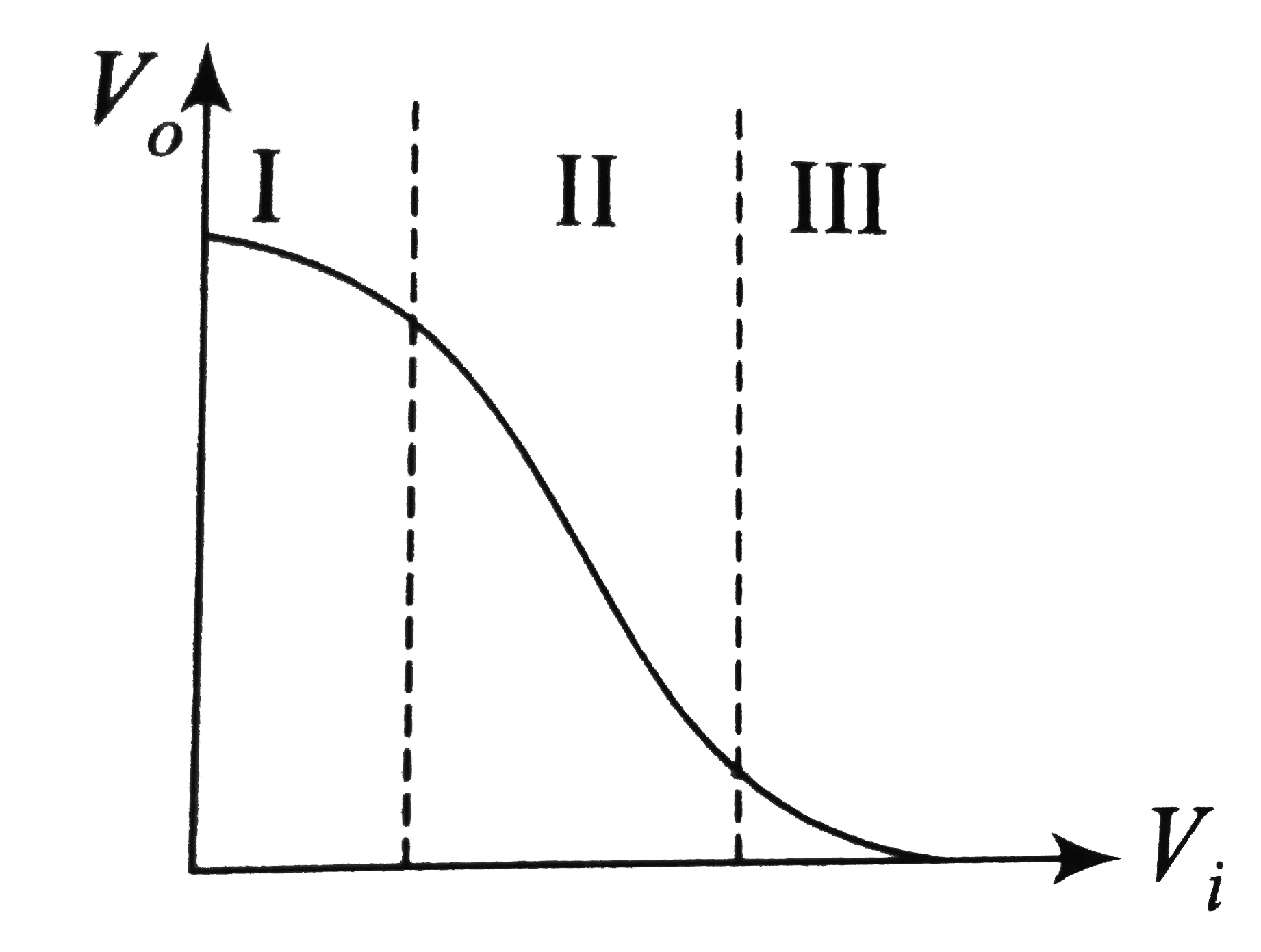
- Transfer characterstics [output voltage (V(o)) vs. input voltage (V(i)...
Text Solution
|
- Transfer characterstics [output voltage (V(o)) vs. input voltage (V(i)...
Text Solution
|
- In the circuit shown in the figure, the input voltage V(i) is 20V,V(BE...
Text Solution
|
- Draw the transfer characteristic curve of a base biased transistor in ...
Text Solution
|
- In a voltage regulating of zener diode, the graph of output voltage v(...
Text Solution
|
- Which is correct for the graph ?
Text Solution
|
- In the circuit shown in the figure, the input voltage V(i) is 20V, V(B...
Text Solution
|
- In the circuit shown in figure, when the input voltage of the base res...
Text Solution
|
- In the given figure, a transistor is connected in common emitter confi...
Text Solution
|