A
B
C
D
Text Solution
Verified by Experts
The correct Answer is:


Topper's Solved these Questions
SEMICONDUCTOR ELECTRONICS: MATERIALS, DEVICES AND SIMPLE CIRCUITS
AAKASH INSTITUTE ENGLISH|Exercise Assignment (Section -B (Objective type question (one option is correct))|29 VideosSEMICONDUCTOR ELECTRONICS: MATERIALS, DEVICES AND SIMPLE CIRCUITS
AAKASH INSTITUTE ENGLISH|Exercise Assignment (Section -C(Linked comprehension type question))|3 VideosSEMICONDUCTOR ELECTRONICS: MATERIALS, DEVICES AND SIMPLE CIRCUITS
AAKASH INSTITUTE ENGLISH|Exercise Try yourself|20 VideosSEMICONDUCTOR ELECTRONICS (MATERIAL, DEVICES AND SIMPLE CIRUITS )
AAKASH INSTITUTE ENGLISH|Exercise Assignment SECTION - D (Assertion & reason type Question)|10 VideosSYSTEM OF PARTICLES AND ROTATIONAL MOTION
AAKASH INSTITUTE ENGLISH|Exercise Try Yourself|63 Videos
Similar Questions
Explore conceptually related problems
AAKASH INSTITUTE ENGLISH-SEMICONDUCTOR ELECTRONICS: MATERIALS, DEVICES AND SIMPLE CIRCUITS-Assignment (Section -A (Objective Type question (One option is correct))
- In an n-p-n transistor, the collector current is 10 mA. If 90% of the ...
Text Solution
|
- Application of forward bias to p-n junction
Text Solution
|
- Intrinsic semiconductor at absolute zero temperature is a
Text Solution
|
- An NPN-transistor circuit is arranged as shown in figure. It is
Text Solution
|
- Four equal resistors, each of resistance 10 ohm are connected as shown...
Text Solution
|
- In a semiconducting material the mobilities of electrons and holes are...
Text Solution
|
- Which of the following gate is called universal gate
Text Solution
|
- A full wave rectifier circuit along with the input and output are show...
Text Solution
|
- In a p-n junction diode having depletion layer of thickness 10^(-6)m, ...
Text Solution
|
- What is the voltage gain in a common emitter amplifier, where output r...
Text Solution
|
- Barrier potential of a p-n junction diode does not depend on -
Text Solution
|
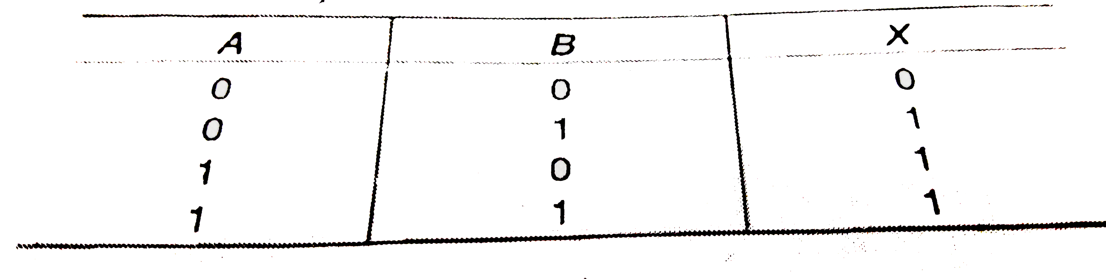
- The following truth table corresponds to the logic gate
Text Solution
|
- Which of the following is not equal to 1 in Boolean algebra ?
Text Solution
|
- Potential barrier developed in a junction diode opposes the flow of
Text Solution
|
- Which of the following diodes is used in unbiased condition ?
Text Solution
|
- Which of the following materials can be used for making solar cell ?
Text Solution
|
- If a full wave rectifier circuit is operating from 50 Hz mains, the fu...
Text Solution
|
- A transistor cannot be used as an
Text Solution
|
- The P-N junction is-
Text Solution
|
- What is the value of output voltage V(0) in the circuit shown in the f...
Text Solution
|