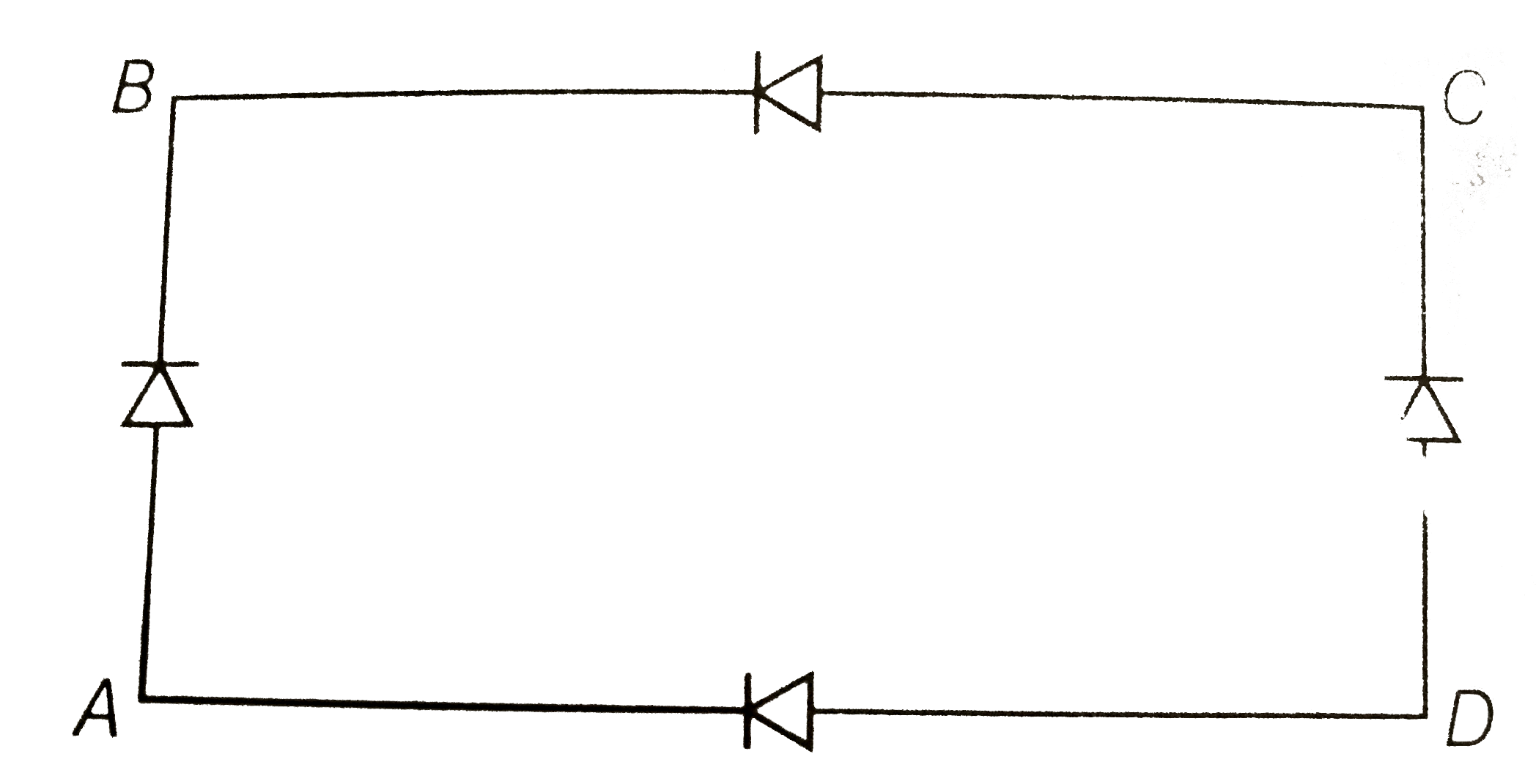
A
B
C
D
Text Solution
Verified by Experts
The correct Answer is:


Topper's Solved these Questions
SEMICONDUCTOR ELECTRONICS: MATERIALS, DEVICES AND SIMPLE CIRCUITS
AAKASH INSTITUTE ENGLISH|Exercise Assignment (Section -C(Linked comprehension type question))|3 VideosSEMICONDUCTOR ELECTRONICS: MATERIALS, DEVICES AND SIMPLE CIRCUITS
AAKASH INSTITUTE ENGLISH|Exercise Assignment (Section-D (Assertion and reason))|5 VideosSEMICONDUCTOR ELECTRONICS: MATERIALS, DEVICES AND SIMPLE CIRCUITS
AAKASH INSTITUTE ENGLISH|Exercise Assignment (Section -A (Objective Type question (One option is correct))|50 VideosSEMICONDUCTOR ELECTRONICS (MATERIAL, DEVICES AND SIMPLE CIRUITS )
AAKASH INSTITUTE ENGLISH|Exercise Assignment SECTION - D (Assertion & reason type Question)|10 VideosSYSTEM OF PARTICLES AND ROTATIONAL MOTION
AAKASH INSTITUTE ENGLISH|Exercise Try Yourself|63 Videos
Similar Questions
Explore conceptually related problems
AAKASH INSTITUTE ENGLISH-SEMICONDUCTOR ELECTRONICS: MATERIALS, DEVICES AND SIMPLE CIRCUITS-Assignment (Section -B (Objective type question (one option is correct))
- An n-type semiconductor has donor levels at 500 meV above the valence ...
Text Solution
|
- In a common emitter amplifier , when a signal of 40 mV is added to the...
Text Solution
|
- The output of the given logica gate is
Text Solution
|
- Two identical capacitors A and B are charged to the same potential V a...
Text Solution
|
- The relationship between alpha and beta is given by
Text Solution
|
- Two identical p-n junctions may be connected in series in which a batt...
Text Solution
|
- In a silicon transistor, a change of 7.89 mA in the emitter current pr...
Text Solution
|
- In a doped semiconductor, the impurity level is 40 meV above the valen...
Text Solution
|
- In figure the input is across the terminals A and C and the output is ...
Text Solution
|
- In the given figure, a transistor is connected in common emitter confi...
Text Solution
|
- A transistor is used in Common-emitter mode in an amplifier circuits. ...
Text Solution
|
- In the given circuit, calculate the ratio of currents through the batt...
Text Solution
|
- In a transistor the current amplification alpha is '0.9', when connect...
Text Solution
|
- A transistor is connected in common base configuration, the collector ...
Text Solution
|
- In the given circuit , the voltage across the base emitter junction is
Text Solution
|
- If the current amplification factor for a transistor connected in comm...
Text Solution
|
- In doped semiconductor one dopent atom is kept typically for how many ...
Text Solution
|
- In a p-n junction diode the value of drift current through depletion r...
Text Solution
|
- In the Boolean algebra bar(A).bar(B) equals
Text Solution
|
- In the adder circuits of two inputs
Text Solution
|