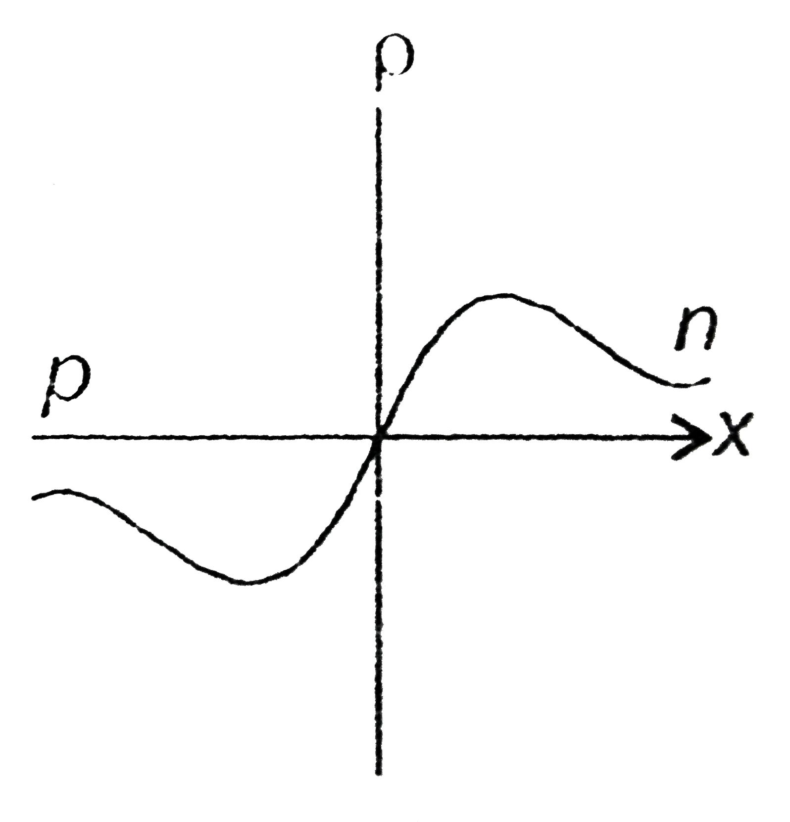
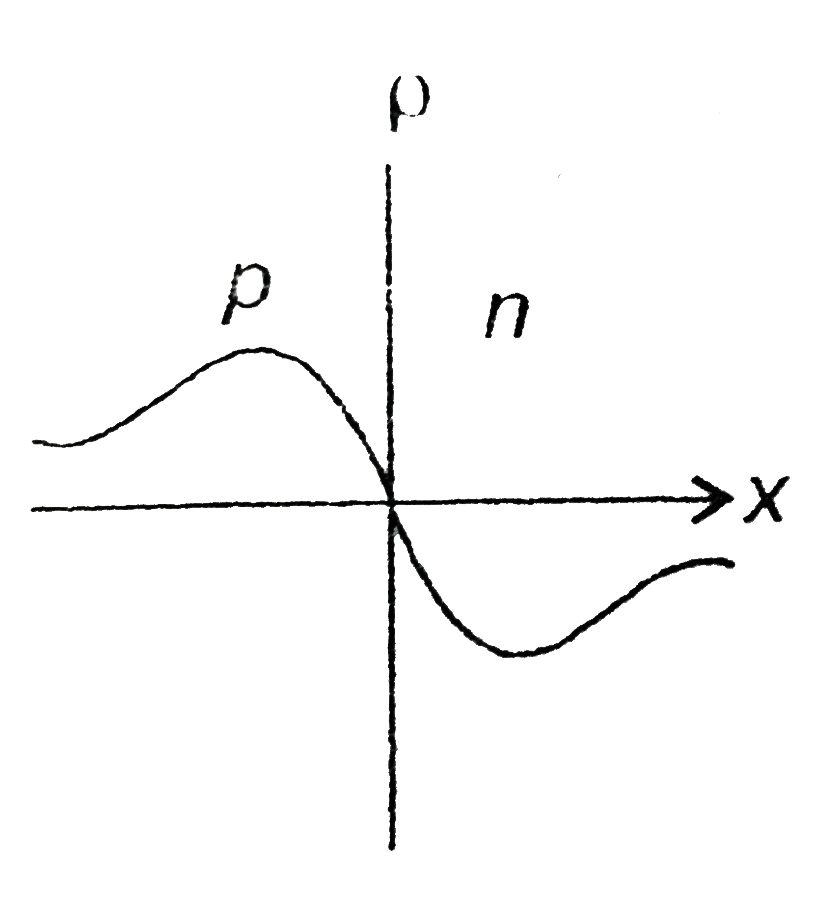
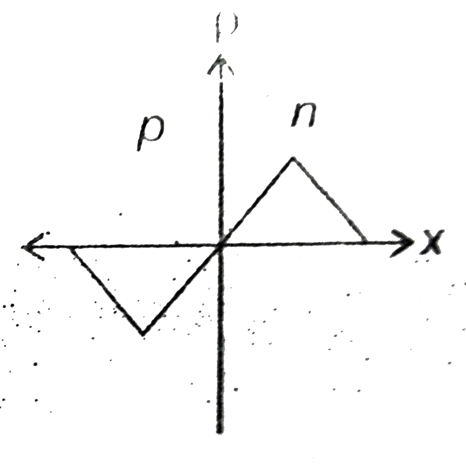
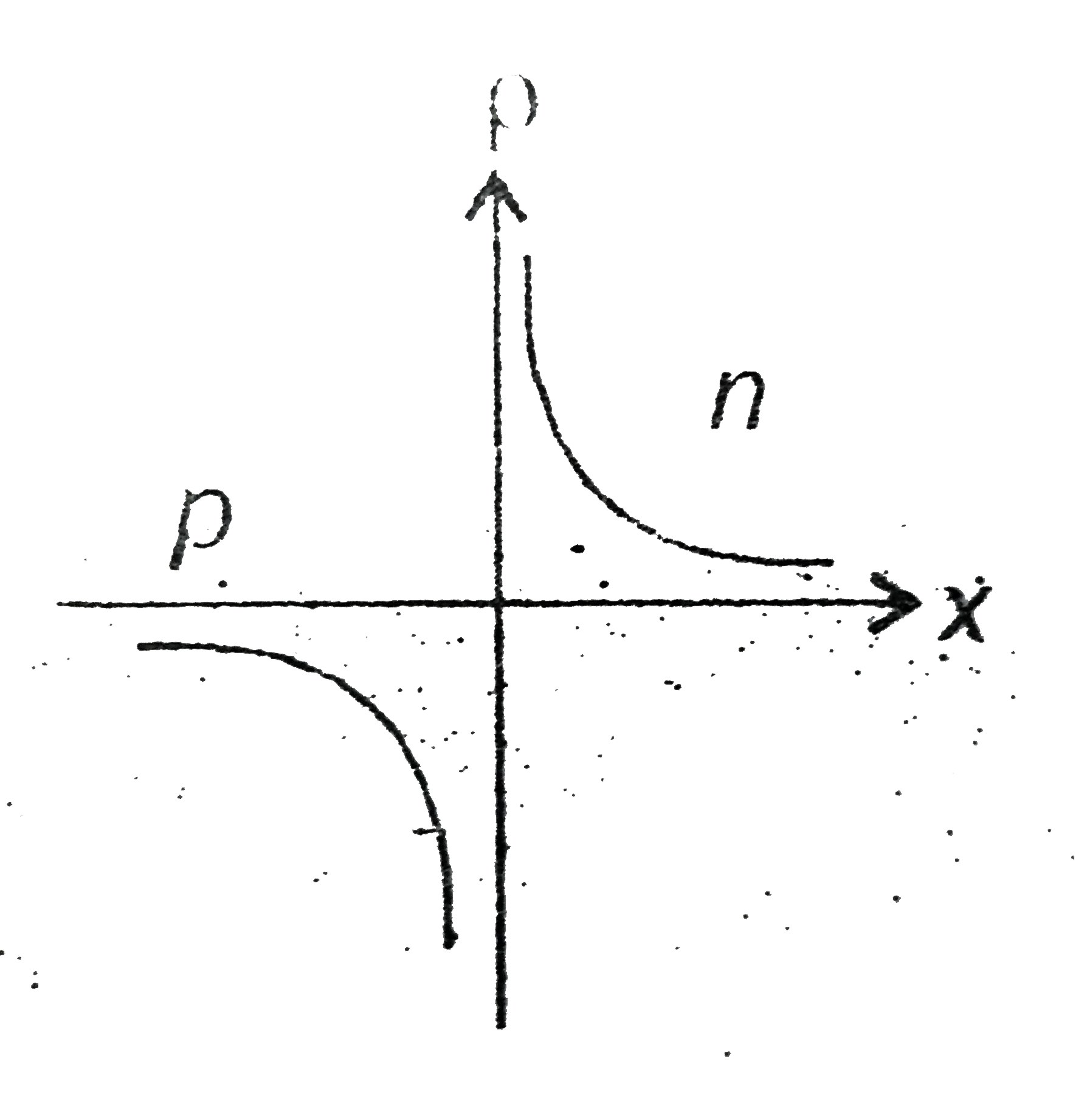
Home
Class 12
PHYSICS
In p-n junction diode, near junction hol...

In p-n junction diode, near junction holes combine with electrons, and impurity ions form a barrier potential which opposes the recombination of electron-hole pairs. Value of barriers potential for Si is 0.7 volt and for Ge is 0.3 V. thus charge density at the junction becomes zero and an electric field is produced near junction. this region is called depletion layer. Thickness of depletion layer is of the order of `10^(-6)` meter. in forward bias p terminal is connected with the positive terminal of cell and n is connected with negative terminal of cell and n is connected with negative terminal of cell. as forward voltage is increased, current increases exponentially.
Correct graph for variation of charge density with distance from the junction is

A

B

C

D

Text Solution

Verified by Experts

The correct Answer is:
A
Promotional Banner

Topper's Solved these Questions

  • SEMICONDUCTOR ELECTRONICS: MATERIALS, DEVICES AND SIMPLE CIRCUITS

    AAKASH INSTITUTE ENGLISH|Exercise Assignment (Section-D (Assertion and reason))|5 Videos
  • SEMICONDUCTOR ELECTRONICS: MATERIALS, DEVICES AND SIMPLE CIRCUITS

    AAKASH INSTITUTE ENGLISH|Exercise Assignment (Section -B (Objective type question (one option is correct))|29 Videos
  • SEMICONDUCTOR ELECTRONICS (MATERIAL, DEVICES AND SIMPLE CIRUITS )

    AAKASH INSTITUTE ENGLISH|Exercise Assignment SECTION - D (Assertion & reason type Question)|10 Videos
  • SYSTEM OF PARTICLES AND ROTATIONAL MOTION

    AAKASH INSTITUTE ENGLISH|Exercise Try Yourself|63 Videos

Similar Questions

Explore conceptually related problems

In p-n junction diode, near junction holes combine with electrons, and impurity ions form a barrier potential which opposes the recombination of electron-hole pairs. Value of barriers potential for Si is 0.7 volt and for Ge is 0.3 V. thus charge density at the junction becomes zero and an electric field is produced near junction. this region is called depletion layer. Thickness of depletion layer is of the order of 10^(-6) meter. in forward bias p terminal is connected with the positive terminal of cell and n is connected with negative terminal of cell and n is connected with negative terminal of cell. as forward voltage is increased, current increases exponentially. As forward voltage is increased barrier potential in p-n junction diode is A. increased B. Decreased C. remain same D. nothing can be said.

In p-n junction diode, near junction holes combine with electrons, and impurity ions form a barrier potential which opposes the recombination of electron-hole pairs. Value of barriers potential for Si is 0.7 volt and for Ge is 0.3 V. thus charge density at the junction becomes zero and an electric field is produced near junction. this region is called depletion layer. Thickness of depletion layer is of the order of 10^(-6) meter. in forward bias p terminal is connected with the positive terminal of cell and n is connected with negative terminal of cell and n is connected with negative terminal of cell. as forward voltage is increased, current increases exponentially. For Si diode minimum required forward voltage so that current can flow is

In a PN -junction diode

p-n junction diode can be used as

The P-N junction is-

In junction diode, the holes are due to

The value of barrier potential of P-N juntion in Ge is-

In a p- n junction diode not connected to any circuit,

In a p-n junction diode, the barrier potential opposes diffusion of

In a p-n junction, depletion region contains