A
B
C
D
Text Solution
Verified by Experts
The correct Answer is:


Similar Questions
Explore conceptually related problems
Recommended Questions
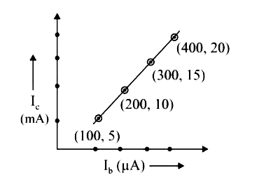
- The transfer characteristic curve of a transistor, having input and ou...
Text Solution
|
- Power gain for N-P-N transistor is 10^(@) , input resistance 100Omega ...
Text Solution
|
- The current gain of a transistor in a common base arrangement is 0.95....
Text Solution
|
- If beta, RL and r are the ac current gain, load resistance and the inp...
Text Solution
|
- If beta, R(L) and r are the AC current gain, load resistance and the i...
Text Solution
|
- The transfer characteristic curve of a transistor, having input and ou...
Text Solution
|
- A common emitter amplifier has a voltage gain of 50, an input impedanc...
Text Solution
|
- यदि CE विन्यास में beta, R(L) एवं r क्रमशः ट्रांजिस्टर के ac धारा लाभ,...
Text Solution
|
- किसी ट्रांजिस्टर के निवेश तथा निर्गम प्रतिरोध क्रमशः 100 Omega तथा 100...
Text Solution
|