A
B
C
D
Text Solution
Verified by Experts
The correct Answer is:


Topper's Solved these Questions
Similar Questions
Explore conceptually related problems
PHYSICS WALLAH-SEMICONDUCTOR ELECTRONICS -NEET PAST 5 YEAR QUESTION
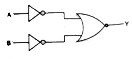
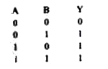
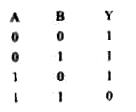
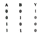
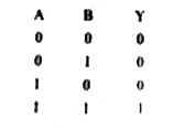
- For the logic circuit shown, the truth table is
Text Solution
|
- The increase in the width of the depletion region in a p-n junction di...
Text Solution
|
- The solids which have negative temperature coefficient of resistance a...
Text Solution
|
- For transistor action, which of the following statements are correct ?
Text Solution
|
- Which of the following gate is called universal gate
Text Solution
|
- Out of following which one is a forward biased diode
Text Solution
|
- A npn transistor is connectedin CEC in which collector voltage drop ac...
Text Solution
|
- Intrinsic semiconductor is converted into ntype extrinsic semiconducto...
Text Solution
|
- The correct boolean operation represented by the circuit diagram drawn...
Text Solution
|
- For a p-type semiconductor, which of the following statements is true?
Text Solution
|
- In the circuit shown in the figure, the input voltage V(i) is 20V,V(BE...
Text Solution
|
- In a p-n junction diode, change in temperature due to heating
Text Solution
|
- In the combination of the following gates the output Y can be written ...
Text Solution
|
- Which of the following represents forward biase diode?
Text Solution
|
- the given electrical network is equivalent to
Text Solution
|
- In a common emitter transistor amplifier the audio signal voltage acro...
Text Solution
|
- Two sides of a semiconductor germanium crystal A and B are doped with ...
Text Solution
|
- From the circuit of the following logic gates, the basic logic gate ob...
Text Solution
|
- A common emitter amplifier circuit is shown in the figure below. For t...
Text Solution
|
- The given circuit has two ideal diodes connected as show in the figure...
Text Solution
|