Home
Class 11
PHYSICS
In the cuircuit shown here the transisto...

In the cuircuit shown here the transistor used has a current gain `beta=100`. What should be the bias resistor `R_(BE)` so that `V_(CE)=5V("neglect "V_(BE))`

A

`1 xx 10^(3) Omega`

B

500

C

`200 xx 10^(3) Omega`

D

`2 xx 10^(3) Omega`

Text Solution

Verified by Experts

The correct Answer is:
C

`I_(C)=(V_(C C)-V_(CE))/(R_(C))=(10-5)/(1kOmega)=5mA`
`rArrV_(C C)=I_(B)R_(B)=(I_(C))/(beta)R_(B)`
`rArrR_(B)=(beta.V_(C C))/(I_(C))=(100xx10)/(5mA)=200 kOmega`
Promotional Banner

Topper's Solved these Questions

  • SEMICONDUCTORS

    ALLEN |Exercise Part-3(Exercise-3)|27 Videos
  • SEMICONDUCTORS

    ALLEN |Exercise Part-3(Exercise-4)|50 Videos
  • SEMICONDUCTORS

    ALLEN |Exercise Part-3(Exercise-1)|84 Videos
  • PHYSICAL WORLD, UNITS AND DIMENSIONS & ERRORS IN MEASUREMENT

    ALLEN |Exercise EXERCISE-IV|7 Videos
  • WAVES AND OSCILLATIONS

    ALLEN |Exercise Part-1(Exercise-05)[B]|42 Videos

Similar Questions

Explore conceptually related problems

In the circuit shown in figure, when the input voltage of the base resistance is 10V, V_(BE) is zero and V_(CE) is also zero. Find the values of I_(B), I_(C ) and beta .

In the following common emitter configuration an NPN transistor with current gain beta=100 is used. The output voltage of the amlifier will be

In the given transistor circuit, the base current is 35 muA . The value of R_(alpha) is V_(AB) is assumed to negiligible :-

In the circuit shown here, what is the value of the unknown resistor R so that the total resistance of the circuit between points P and Q is also equal to R

Consider the circuit arrangement shown in figure (1) for studying input and output characteristics of n-p-n transistor in CE configuration. Select the values of R_(B) and R_(C ) for a transistor whose V_(BE)=0.7V , so that the transistor is operating at point Q as shown in the characteristics shown in figure (2). Given that the input impedance of the transistor is very small and V_(C C)=V_(BB)=16V , also find the voltage gain and power gain of circuit making appropriate assumptions.

5 In a Zener regulated power supply a Zener diode with V_(Z) = 6.0 V is used for regulation. The load current is to be 4.0 mA and the unregulated input is 10.0 V. What should be the value of series resistor R_(S) ?

In a Zener regulated power supply a Zener diode with V_(Z)=6.0V is used for regulation. The load current is to be 4.0 mA and the unregulated input is 10.0V. What should be the value of series resistor R_(S) ?

A bettery of emf 10 V and internal resistacne 3 Omega is connected to a resistor. If the current in the circuit is 0.5A, what is the resistance of the resistor ? What is the terminal voltage of the bettery when the circuit is closed ?

A change of 0.04 V takes place between the base and the emitter when an input signal is connected to the CE transistor amplifier. As a result, 2014 change take place in the base current and a change of 2 mA lakes place in the collector current. Find the input resistance and A.C. current gain.

ALLEN -SEMICONDUCTORS-Part-3(Exercise-2)
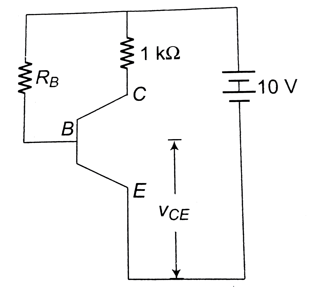
  1. In the following common emitter configuration an NPN transistor with c...

    Text Solution

    |

  2. In the given transistor circuit, the base current is 35 muA. The value...

    Text Solution

    |

  3. In the cuircuit shown here the transistor used has a current gain beta...

    Text Solution

    |

  4. Choose the only false statement from the following.

    Text Solution

    |

  5. What will be conductance of pure silicon crystal at 300 K Temp. If ele...

    Text Solution

    |

  6. The output of the given logic gate is 1 when inputs A,B and C are such...

    Text Solution

    |

  7. The arrangement shown in figure performs the logic function of a/an….g...

    Text Solution

    |

  8. You are given two circuits as shown in following figure. The logic ope...

    Text Solution

    |

  9. Which of the following Boolean expression is not correct :-

    Text Solution

    |

  10. Which of the following relation is valid in Boolean algebra :-

    Text Solution

    |

  11. Given below are four logic tage symboles. Those for OR, NOR and NAND a...

    Text Solution

    |

  12. The output Y of the combination of gates shown in equal to :-

    Text Solution

    |

  13. Which of the following relation is valid in Boolean algebra :-

    Text Solution

    |

  14. The diagram of a logic circuit is given below. The output F of the cir...

    Text Solution

    |

  15. The following configuration of gate is equivalent to

    Text Solution

    |

  16. To get an output of 1 form the circuit shown in figure the input must ...

    Text Solution

    |

  17. The circuit shown here is logically equivalent to :-

    Text Solution

    |

  18. Which of the following will have an output of 1 :-

    Text Solution

    |

  19. The logic symbols shown here are logically equivalent to :-

    Text Solution

    |

  20. The combination of the gates shown will produce

    Text Solution

    |