In practice , the AND gate is realised with the help of the electrons circuit using two diodes `D_(1)` and `D_(2)` as show in Fig. The two diodes play the roles of the switches A and B as explained below .
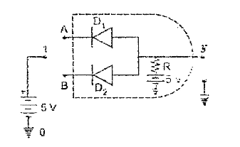
(a) A = 0 and B = 0 . Both the diodes `D_(1)` and `D_(2)` get forward biased and hence condcut . The output y will be the voltage drop acrooss `D_(1)` or `D_(2)` . Since diodes are ideal , no voltage drop occurs across the diodes . Hence , the output y is 0.
(b) A =1 and B = 0 . The diode `D_(2)` will conduct and diode `D_(1)` will remain idle . Now , output y is voltage across `D_(2)` and hence it is 0.
(c) A = 0 and B = I . The diode `D_(1)` will conduct , while `D_(2)` will not conduct . Now , output y is voltage across `D_(1)` , which is 0.
(d) A =1 and B =1 . Both the diodes will not conduct . The output y will equal battery voltage 5 V i.e., equal to 1.
These result in the four case are same as listed in Table 3.03 in the form of truth table of the AND gate .


