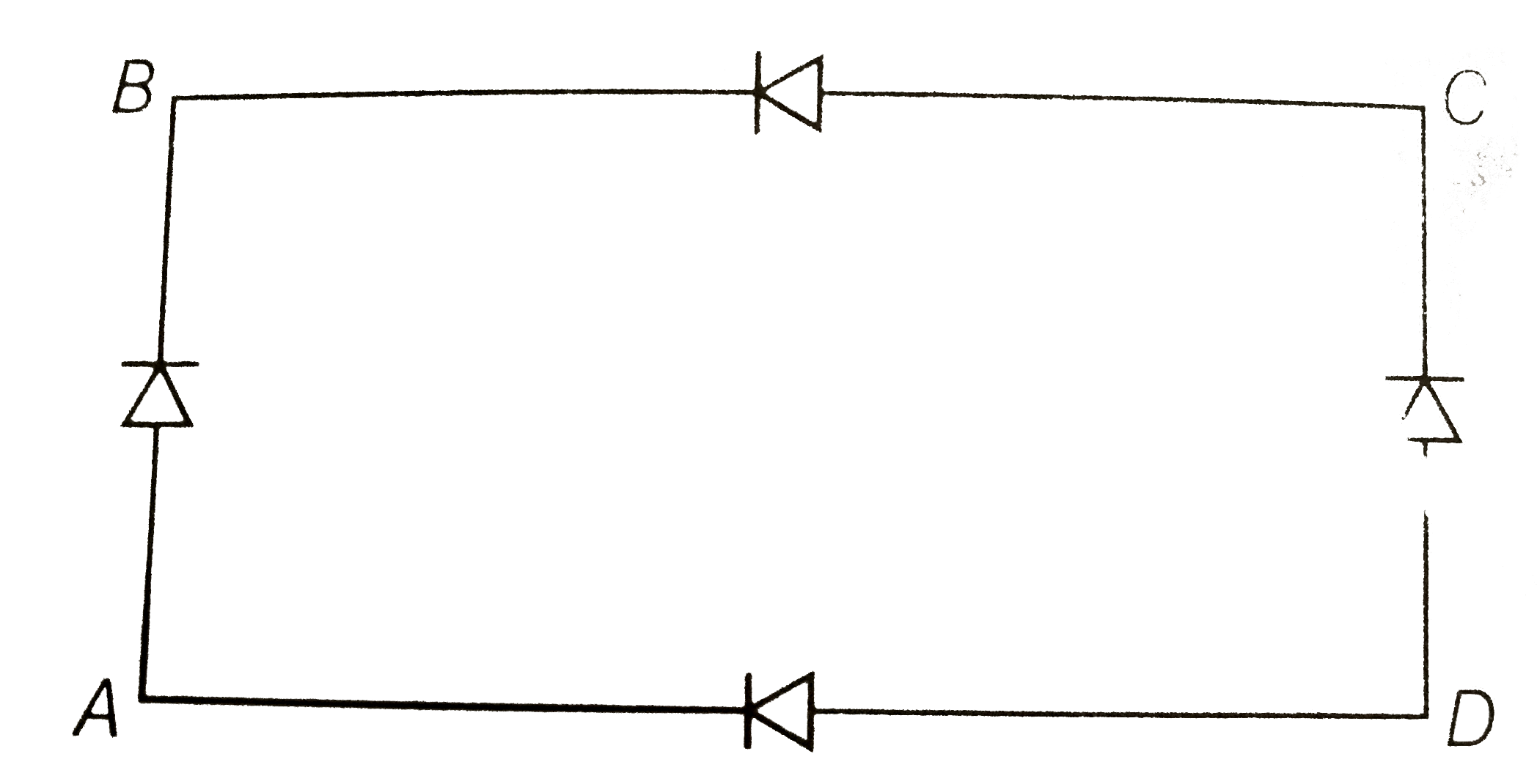
A
B
C
D
Text Solution
Verified by Experts
The correct Answer is:


Topper's Solved these Questions
SEMICONDUCTORS
ALLEN|Exercise Part-3(Exercise-3)|27 VideosSEMICONDUCTORS
ALLEN|Exercise Part-3(Exercise-4)|51 VideosSEMICONDUCTORS
ALLEN|Exercise Part-3(Exercise-1)|84 VideosPHYSICAL WORLD, UNITS AND DIMENSIONS & ERRORS IN MEASUREMENT
ALLEN|Exercise EXERCISE-IV|8 VideosWAVES AND OSCILLATIONS
ALLEN|Exercise Part-1(Exercise-05)[B]|42 Videos
Similar Questions
Explore conceptually related problems
ALLEN-SEMICONDUCTORS-Part-3(Exercise-2)
- A diode made forward biased by a two volt battery however there is a d...
Text Solution
|
- Forbidden energy gap of Ge is 0.75eV, maximum wave length of incident ...
Text Solution
|
- In figure the input is across the terminals A and C and the output is ...
Text Solution
|
- An oscillator is nothing but an amplifier with
Text Solution
|
- In the following common emitter configuration an npn transistor with c...
Text Solution
|
- In the given transistor circuit, the base current is 35 muA. The value...
Text Solution
|
- In the circuit shown here, the transistor used has a current gain beta...
Text Solution
|
- Choose the false statement from the following.
Text Solution
|
- What will be conductivity of pure sillicon crystal at 300 K temp? if e...
Text Solution
|
- The output of the given logic gate is 1 when inputs A,B and C are such...
Text Solution
|
- The arrangement shown in figure performs the logic function of a/an….g...
Text Solution
|
- You are given two circuits as shown in Fig. 14.38, which consist of NA...
Text Solution
|
- Which of the following expressions is not true ?
Text Solution
|
- Which of the following relation is valid in Boolean algebra :-
Text Solution
|
- Given below are four logic gates symbols. NAND, NOR and OR are respect...
Text Solution
|
- The output Y of the combination of logic gates shown is equal to
Text Solution
|
- Which of the following relation is valid in Boolean algebra :-
Text Solution
|
- The output of given logic circuit is
Text Solution
|
- The following configuration of gate is equivalent to
Text Solution
|
- To get an output 1 from the circuit shown in the figure, the input mus...
Text Solution
|