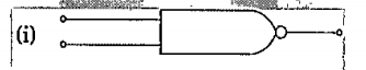
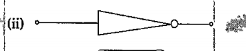
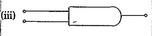
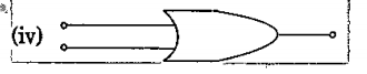
 The logic symbols for OR, NOT and NAND gates are respectively
A
B
C
D
Text Solution
Verified by Experts


Topper's Solved these Questions
Similar Questions
Explore conceptually related problems
SARAS PUBLICATION-ELECTRONIC DEVICES-EXAMPLE
- A p-n photodiode is made of a material with ,band gap of 2.0 ev The mi...
Text Solution
|
- The circuit is equivalent to:
Text Solution
|
- The symbolic representation of four logic gates are given below: ...
Text Solution
|
- A p-n photodiode is farbricated from a semiconductor with a band gap o...
Text Solution
|
- The device that act as a complete electronic circuit is:
Text Solution
|
- In forward biasing of the p-n junction
Text Solution
|
- Symbolic represntation of four logic gates are shown as Pick out...
Text Solution
|
- The figure show a logic circuit with inputs A and B and the output C.T...
Text Solution
|
- C, Si and Ge have same lattice structure . Why is C an insulator while...
Text Solution
|
- For a CE- transistor amplifier , the audio signal voltage across the c...
Text Solution
|
- Two ideal diodes are connected to a battery as shown in the circuit .T...
Text Solution
|
- In a common emiter (CE) amplifier having a voltage gain G, the transis...
Text Solution
|
- The output (X) of the logic circuit shown in figure will be
Text Solution
|
- In an unbiased p-n junction , holes diffuse from the p-region to n- re...
Text Solution
|
- One way in which the operation of a-n-p-n transistor differs from that...
Text Solution
|
- The output from a NAND gate is divided into two in parallel and fed to...
Text Solution
|
- The given graph represents V-I characteristic for semiconductor device...
Text Solution
|
- Which logic gate is represented by the following combination of logic ...
Text Solution
|
- If in a p-n junction,square input signal of 10 V is applied as shown T...
Text Solution
|
- For CE transistor amplifier, the, audio signal voltage across the coll...
Text Solution
|