Home
Class 12
PHYSICS
If in a p-n junction,square input signal...

If in a p-n junction,square input signal of 10 V is applied as shown Then the output across `R_L` will be:

A


B


C


D


Text Solution

Verified by Experts

Promotional Banner

Topper's Solved these Questions

  • ELECTROMAGNETIC WAVES

    SARAS PUBLICATION|Exercise EXAMPLE|15 Videos
  • Electrostatics

    SARAS PUBLICATION|Exercise EXAMPLE|31 Videos

Similar Questions

Explore conceptually related problems

A full - wave rectifier circuit with an ac input is shown. The output voltage across R_(L) is represented as

Figure shows a typical circuit for low-pass filter. An AC input V_i = 10 mV is applied at the left end and the output V_0 is received at the right end. Find the output voltages for v = 10 kHz, 100 kHz, 1.0 MHz and 10.0 MHz . Note that as the frequency is increased the output decreases and hence the name low-pass filter.

Two capacitors of capacities 100muF and 200muF are connected in sereis. A.p.d. of 90 V is applied across them. Calculate the p..d across each capacitor.

In a common-base amplifier, the phase difference between the input signal voltage and the output voltage (across collector and base) is

In a p-n junction,a potential barrier of 250 mev exsists across the junction.A hole with a kimetic energy of 300 meV approaches the junction. Find the kinetic energy of the hole when it crosses the junction if the hole approached the junction (a)from the p-side and (b)from the n-side.

A mass of 6kg is suspended by a rope of length 2m from a celling a force of 50N in the horizontal direction is applied at the midpoint of the rope as shown in the figure what is the angle the rope makes with the vertical is equalibrium take g=10 ms^(-2) neglect mass of the rope

When a forward bias is applied to a p-n junction , it

SARAS PUBLICATION-ELECTRONIC DEVICES-EXAMPLE
  1. The figure show a logic circuit with inputs A and B and the output C.T...

    Text Solution

    |

  2. C, Si and Ge have same lattice structure . Why is C an insulator while...

    Text Solution

    |

  3. For a CE- transistor amplifier , the audio signal voltage across the c...

    Text Solution

    |

  4. Two ideal diodes are connected to a battery as shown in the circuit .T...

    Text Solution

    |

  5. In a common emiter (CE) amplifier having a voltage gain G, the transis...

    Text Solution

    |

  6. The output (X) of the logic circuit shown in figure will be

    Text Solution

    |

  7. In an unbiased p-n junction , holes diffuse from the p-region to n- re...

    Text Solution

    |

  8. One way in which the operation of a-n-p-n transistor differs from that...

    Text Solution

    |

  9. The output from a NAND gate is divided into two in parallel and fed to...

    Text Solution

    |

  10. The given graph represents V-I characteristic for semiconductor device...

    Text Solution

    |

  11. Which logic gate is represented by the following combination of logic ...

    Text Solution

    |

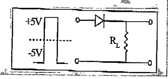
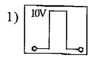
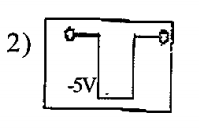
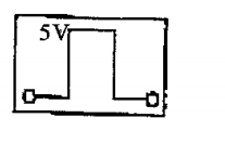
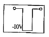
  12. If in a p-n junction,square input signal of 10 V is applied as shown T...

    Text Solution

    |

  13. For CE transistor amplifier, the, audio signal voltage across the coll...

    Text Solution

    |

  14. What is the output Y in the following circuit , When all the three inp...

    Text Solution

    |

  15. To get output 1 for the following circuit, the correct choice for the ...

    Text Solution

    |

  16. A small signal voltage V(t)=V0 sin omegat is applied across an ideal c...

    Text Solution

    |

  17. Consider the junction diode as ideal. The value of current flowing thr...

    Text Solution

    |

  18. A npn transistor is cnnected in common emitter configuration in a give...

    Text Solution

    |

  19. The given electrial network is equivalenf to:

    Text Solution

    |

  20. Which of the following represent forward bias diode ?

    Text Solution

    |