Home
Class 12
PHYSICS
Assume that the silicon diode in the cir...

Assume that the silicon diode in the circui shown in fig. requires a minimum current of 1mA to be above the knee point (0.7V) of its I-V characteristics. Aslo assume that the voltage across the diode is independent of current above the knee point.
If `R=1kOmega`, what is the minimum voltage` V_(B)` required to keep the diode above the knee point?

Promotional Banner

Topper's Solved these Questions

  • SEMICONDUCTOR DEVICES

    MODERN PUBLICATION|Exercise EXERCISE|174 Videos
  • REFRACTION OF LIGHT

    MODERN PUBLICATION|Exercise EXERCISE|168 Videos
  • Solids

    MODERN PUBLICATION|Exercise EXERCISE|66 Videos

Similar Questions

Explore conceptually related problems

Assume that the silicon diode in the circui shown in fig. requires a minimum current of 1mA to be above the knee point (0.7V) of its I-V characteristics. Aslo assume that the voltage across the diode is independent of current above the knee point. If V_(B)=5 V, what should be the maximum value of R so that the voltage is above the knee point?

Assume that the silicon diode in the circui shown in fig. requires a minimum current of 1mA to be above the knee point (0.7V) of its I-V characteristics. Aslo assume that the voltage across the diode is independent of current above the knee point. If V_(B)=5V , what should be the value of R to estabilish the current of 5mA in the circuit?

Assume that the silicon diode in the circui shown in fig. requires a minimum current of 1mA to be above the knee point (0.7V) of its I-V characteristics. Aslo assume that the voltage across the diode is independent of current above the knee point. What is the power dissipated in the resistance R and in the diode, when a current of 5mA flows in the circuit at V_(B)=6V ?

In figure what is the voltage needed to maintain 15V across the load resistance R_(L) of 2K, assuming that the series resistance R is 200 Omega and the zener requires a minimum current of 10mA to work satisfactorily? What is the zener rating required?

The diode used in the circuit shown in the adjacent figure has a constant voltage drop of 0.5V at all currents and a maximum power rating of 100mW.What should be the value of resistor R connected in series with the diode for obtaining maximum current?

In the circuit shown in Fig. EP. 14.7, if the diode forward voltage drop is 0.3 V, the voltage differnece between A and B is

Figure 3.33 shows a potentiometer with a cell of 2.0 V and internal resistance 0.40 Omega maintaining a potential drop across the resistor wire AB. A standard cell which maintains a constant emf of 1.02 V (for very moderate currents upto a few mA) gives a balance point at 67.3 cm length of the wire. To ensure very low currents drawn from the standard cell, a very high resistance of 600 k Omega is put in series with it, which is shorted close to the balance point. The standard cell is then replaced by a cell of unknown emf epsilon and the balance point found similarly, turns out to be at 82.3 cm length of the wire. Would the method work in the above situation if the driver cell of the potentiometer had an emf of 1.0V instead of 2.0V? :

Figure shows a potentiometer with a cell of 2.0 V and internal resistance 0.40 Omega maintaining a potential drop across the resistor wire AB. A standard cell which maintains a constant emf of 1.02 V (for very moderate currents upto a few mA) gives a balance point at 67.3 cm length of the wire. To ensure very low currents drawn from the standard cell, a very high resistance of 600 k Omega is put in series with it, which is shorted close to the balance point. The standard cell is then replaced by a cell of unknown emf epsilon and the balance point found similarly, turns out to be at 82.3 cm length of the wire. What purpose does the high resistance of 600 kOmega have? :

Figure 3.33 shows a potentiometer with a cell of 2.0 V and internal resistance 0.40 Omega maintaining a potential drop across the resistor wire AB. A standard cell which maintains a constant emf of 1.02 V (for very moderate currents upto a few mA) gives a balance point at 67.3 cm length of the wire. To ensure very low currents drawn from the standard cell, a very high resistance of 600 k Omega is put in series with it, which is shorted close to the balance point. The standard cell is then replaced by a cell of unknown emf epsilon and the balance point found similarly, turns out to be at 82.3 cm length of the wire. Is the balance point affected by the internal resistance of the driver cell?:

MODERN PUBLICATION-SEMICONDUCTOR DEVICES-EXERCISE
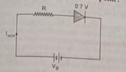
  1. Assume that the silicon diode in the circui shown in fig. requires a m...

    Text Solution

    |

  2. Explain the two processes involved in the formation of a p-n junciton ...

    Text Solution

    |

  3. Describe briefly, with the help of a diagram, the role of the two impo...

    Text Solution

    |

  4. What do you mean by depletion region in a p-n junction ?

    Text Solution

    |

  5. Explain the terms depletion layer and potential barrier for a junction...

    Text Solution

    |

  6. Explain the terms depletion layer and potential barrier for a junction...

    Text Solution

    |

  7. Explain the two processes involved in the formation of a p-n junciton ...

    Text Solution

    |

  8. Explain forward bias and reverse bias of the junction diode.

    Text Solution

    |

  9. Explain forward bias and reverse bias of the junction diode.

    Text Solution

    |

  10. Explain forward bias and reverse bias of the junction diode.

    Text Solution

    |

  11. With the help of circuit diagram, explain theV-l characteristics of p-...

    Text Solution

    |

  12. Draw a circuit diagram with a p-n junction in forward bias.

    Text Solution

    |

  13. With the help of circuit diagram, explain theV-l characteristics of p-...

    Text Solution

    |

  14. Draw a circuit diagram with a p-n junction in forward bias.

    Text Solution

    |

  15. Explain with the help of circuit diagram, how V-l characteristics of p...

    Text Solution

    |

  16. With the help of circuit diagram, explain theV-l characteristics of p-...

    Text Solution

    |

  17. Define the term dynamic resistance of a p-n junction diode.

    Text Solution

    |

  18. Define Rectification. With the help a circuit diagram explain the work...

    Text Solution

    |

  19. With the help of circuit diagram explain working of junction diode as ...

    Text Solution

    |

  20. Draw the circuit diagram of a half wave rectifier using a junction dio...

    Text Solution

    |

  21. Draw the circuit diagram of a half wave rectifier using a junction dio...

    Text Solution

    |