Topper's Solved these Questions
Similar Questions
Explore conceptually related problems
MODERN PUBLICATION-SEMICONDUCTOR DEVICES-EXERCISE
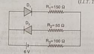
- The circuit shown in the figure contains two diodes each with a forwar...
Text Solution
|
- Explain the two processes involved in the formation of a p-n junciton ...
Text Solution
|
- Describe briefly, with the help of a diagram, the role of the two impo...
Text Solution
|
- What do you mean by depletion region in a p-n junction ?
Text Solution
|
- Explain the terms depletion layer and potential barrier for a junction...
Text Solution
|
- Explain the terms depletion layer and potential barrier for a junction...
Text Solution
|
- Explain the two processes involved in the formation of a p-n junciton ...
Text Solution
|
- Explain forward bias and reverse bias of the junction diode.
Text Solution
|
- Explain forward bias and reverse bias of the junction diode.
Text Solution
|
- Explain forward bias and reverse bias of the junction diode.
Text Solution
|
- With the help of circuit diagram, explain theV-l characteristics of p-...
Text Solution
|
- Draw a circuit diagram with a p-n junction in forward bias.
Text Solution
|
- With the help of circuit diagram, explain theV-l characteristics of p-...
Text Solution
|
- Draw a circuit diagram with a p-n junction in forward bias.
Text Solution
|
- Explain with the help of circuit diagram, how V-l characteristics of p...
Text Solution
|
- With the help of circuit diagram, explain theV-l characteristics of p-...
Text Solution
|
- Define the term dynamic resistance of a p-n junction diode.
Text Solution
|
- Define Rectification. With the help a circuit diagram explain the work...
Text Solution
|
- With the help of circuit diagram explain working of junction diode as ...
Text Solution
|
- Draw the circuit diagram of a half wave rectifier using a junction dio...
Text Solution
|
- Draw the circuit diagram of a half wave rectifier using a junction dio...
Text Solution
|
