A

B
C
D
Text Solution
Verified by Experts
The correct Answer is:


Topper's Solved these Questions
SEMICONDUCTOR DEVICES
AAKASH SERIES|Exercise PRACTICE EXERCISE (TRANSISTORS )|8 VideosSEMICONDUCTOR DEVICES
AAKASH SERIES|Exercise PRACTICE EXERCISE (LOGIC GATES )|15 VideosSEMICONDUCTOR DEVICES
AAKASH SERIES|Exercise EXERCISE -II (LOGIC GATES)|12 VideosRAY OPTICS
AAKASH SERIES|Exercise PROBLEMS ( LEVEL-II)|60 VideosUNITS AND MEASUREMENT
AAKASH SERIES|Exercise PRACTICE EXERCISE|45 Videos
Similar Questions
Explore conceptually related problems
AAKASH SERIES-SEMICONDUCTOR DEVICES-PRACTICE EXERCISE (ENERGY BANDS AND CLASSIFICATION OF SOLIDS )
- The junction diode shown in the figure is ideal. The current in the ci...
Text Solution
|
- The current from below circuit if forward resistance of the diode is 5...
Text Solution
|
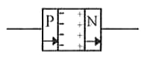
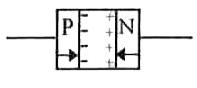
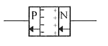
- The diagram correctly represent the direction of flow of charge carrie...
Text Solution
|
- The barrier potential in an ideal P-n junction diode is 0.3 volts. The...
Text Solution
|
- The diode used in figure requires minimum current of ImA to be above t...
Text Solution
|
- Calculate the value of R, if the maximum value of forward current of t...
Text Solution
|
- The potential barrier existing across an unbiased p-n junction is 0.2 ...
Text Solution
|
- In a p-n junction, a potential barrier of 250 meV exists across the ju...
Text Solution
|
- Calculate the current through the circuit and the potential difference...
Text Solution
|
- Find the currents through the resistances in the circuits shown in fig...
Text Solution
|
- Find the currents through the resistances in the circuits shown in fig...
Text Solution
|
- A potential barrier V volts exists across a P-N junction. The thicknes...
Text Solution
|
- The current flow through the resistance in the given circuit is
Text Solution
|
- Consider a p-n junction diode which has a potential drop of 0.5 V whi...
Text Solution
|
- The potential barrier of a P-N junction diode is 50 meV, When an elect...
Text Solution
|
- In a half wave rectifier circuit operating from 50 Hz mains frequency,...
Text Solution
|
- A full-wave rectifier is used to convert 50 Hz A.C into D.C, then the ...
Text Solution
|
- The applied a.c power to a full-wave rectifier is 400W. The d.c power ...
Text Solution
|
- In a half wave rectifier, a p-n junction diode with internal resistanc...
Text Solution
|
- A full wave rectifier circuit along with the output is shown in figure...
Text Solution
|