A
B
C
D
Text Solution
Verified by Experts


Topper's Solved these Questions
SEMICONDUCTOR DEVICES
AAKASH SERIES|Exercise EXERCISE - IB|7 VideosSEMICONDUCTOR DEVICES
AAKASH SERIES|Exercise EXERCISE - II|17 VideosSEMICONDUCTOR DEVICES
AAKASH SERIES|Exercise PROBLEMS|41 VideosRAY OPTICS
AAKASH SERIES|Exercise PROBLEMS ( LEVEL-II)|60 VideosUNITS AND MEASUREMENT
AAKASH SERIES|Exercise PRACTICE EXERCISE|45 Videos
Similar Questions
Explore conceptually related problems
AAKASH SERIES-SEMICONDUCTOR DEVICES-EXERCISE - IA
- In a P-N junction diode which is not connected to any circuit-
Text Solution
|
- The dominant mechanism for motion of charge carriers in forward and re...
Text Solution
|
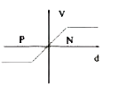
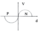
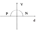
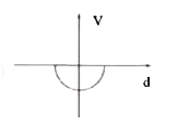
- The correct curve between potential and distance near P-N junction is
Text Solution
|
- Potential barrier developed in a junction diode opposes the flow of
Text Solution
|
- When p-n junction diode is forward biased, then
Text Solution
|
- In the middle of the depletion layer of a reverse-biased p - n junctio...
Text Solution
|
- Avalanche breakdown in a semiconductor diode occurs when-
Text Solution
|
- When a p-n junction diode is reverse biased the flow of current across...
Text Solution
|
- The small currents in reverse biased condition of p-n diode are due to
Text Solution
|
- In a p-n junction diode, change in temperature due to heating
Text Solution
|
- The zener diode can be used as
Text Solution
|
- In an unbiased p-n junction, holes diffuse from the P-region to n-regi...
Text Solution
|
- The I - V characteristic of an LED is
Text Solution
|
- In figure, assuming the diodes to be ideal,
Text Solution
|
- Transistor can be used as :-
Text Solution
|
- A n-p-n transistor conducts when
Text Solution
|
- When a n-p-n transistor is used as an amplifier, then
Text Solution
|
- In a common base amplifier the phase difference the input signal volta...
Text Solution
|
- Transfer characteristic [output voltage (V(0)) vs input voltage (V(i))...
Text Solution
|
- An AND gate
Text Solution
|