A
B
C

D

Text Solution
Verified by Experts
The correct Answer is:


Topper's Solved these Questions
ELECTRONICS
ERRORLESS|Exercise NCERT Based Questions (Junction Transistor)|29 VideosELECTRONICS
ERRORLESS|Exercise NCERT Based Questions (Digital Electronics)|23 VideosELECTRONICS
ERRORLESS|Exercise Assertion & Reason|26 VideosELECTRON, PHOTON, PHOTOELECTRIC EFFECT & X -RAY
ERRORLESS|Exercise ASSERTION & REASON|27 VideosELECTROSTATICS
ERRORLESS|Exercise ASSERTION & REASON|25 Videos
Similar Questions
Explore conceptually related problems
ERRORLESS-ELECTRONICS-NCERT Based Questions (Semiconductor Diode)
- The dominant mechanisms for motion of charge carriers in forward and r...
Text Solution
|
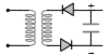
- Which of the following is not a rectifier circuit
Text Solution
|
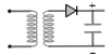
- Which is the correct diagram of a half- wave reactifier?
Text Solution
|
- In the diagram, the input is across the terminals A and C and the outp...
Text Solution
|
- If a full wave rectifier circuit is operating from 50 Hz mains, the fu...
Text Solution
|
- If in a p - n junction diode , a square input signal of 10 V is applie...
Text Solution
|
- A diode is connected to 220V (rms) ac in series with a capacitor as sh...
Text Solution
|
- The output in the circuit of figure is taken across a capacitor. It is...
Text Solution
|
- Two identical capacitors A and B are charged to the same potential V a...
Text Solution
|
- Consider the folllowing statements i and ii and identify the correct c...
Text Solution
|
- Zener diode is used as
Text Solution
|
- Suppose an unregulated D.C. input voltage V(1) is applied to a Zener ...
Text Solution
|
- If the voltage between the terminals A and B is 17V and zener breakdow...
Text Solution
|
- The graph shown in Fig. represents the I-V characteristics of a zener ...
Text Solution
|
- A p-n photodiode is made of a material with a band gap of 2.0 eV. The ...
Text Solution
|
- A certain p-n junction, having a depletion region of width 20 mum, was...
Text Solution
|
- In a forward biased PN- junction diode, the potential barrier in the d...
Text Solution
|
- In Fig . V(0) is the potential barrier across a p-n junction, when no ...
Text Solution
|
- The diode shown in the circuit is a silicon diode. The potential diffe...
Text Solution
|
- A bridge rectifier is shown in figure. Alternating input is given acro...
Text Solution
|