A
B
C
D
Text Solution
Verified by Experts
The correct Answer is:


Topper's Solved these Questions
ELECTRONICS
ERRORLESS|Exercise NCERT Based Questions (Junction Transistor)|29 VideosELECTRONICS
ERRORLESS|Exercise NCERT Based Questions (Digital Electronics)|23 VideosELECTRONICS
ERRORLESS|Exercise Assertion & Reason|26 VideosELECTRON, PHOTON, PHOTOELECTRIC EFFECT & X -RAY
ERRORLESS|Exercise ASSERTION & REASON|27 VideosELECTROSTATICS
ERRORLESS|Exercise ASSERTION & REASON|25 Videos
Similar Questions
Explore conceptually related problems
ERRORLESS-ELECTRONICS-NCERT Based Questions (Semiconductor Diode)
- A certain p-n junction, having a depletion region of width 20 mum, was...
Text Solution
|
- In a forward biased PN- junction diode, the potential barrier in the d...
Text Solution
|
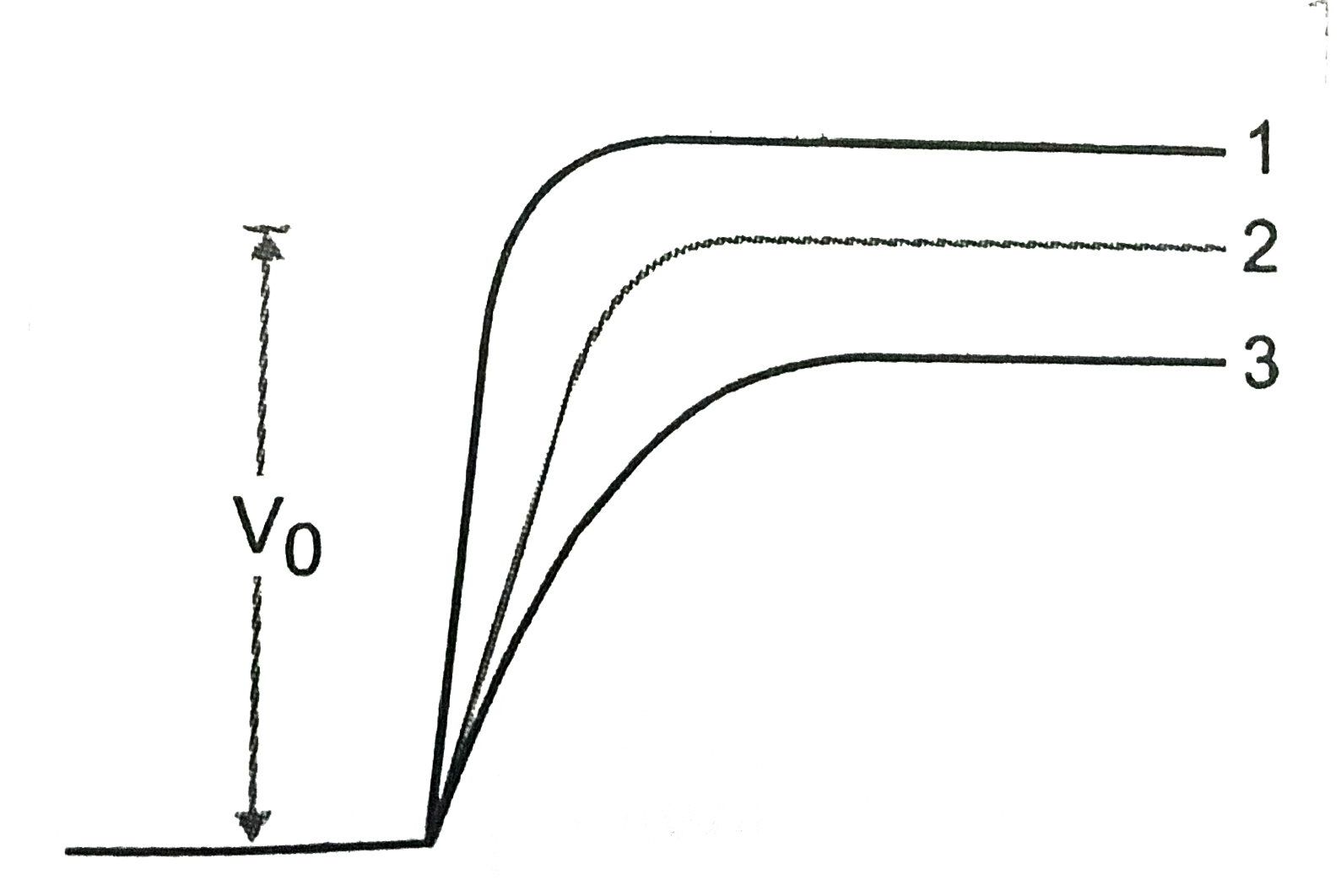
- In Fig . V(0) is the potential barrier across a p-n junction, when no ...
Text Solution
|
- The diode shown in the circuit is a silicon diode. The potential diffe...
Text Solution
|
- A bridge rectifier is shown in figure. Alternating input is given acro...
Text Solution
|
- In the following circuit, the current flowing through 1kOmega. resisto...
Text Solution
|
- In figure given below, assuming the diodes to be ideal
Text Solution
|
- In the given figure, which of the diodes are forward biased
Text Solution
|
- Of the diodes shown in the following figures, which one is reverse bia...
Text Solution
|
- Currents flowing in each of the circuits A and B respectively are
Text Solution
|
- Assuming the diodes to be of silicon with forward resistance zero, the...
Text Solution
|
- The diode used in the circuit shown in the figure has a constant volta...
Text Solution
|
- The junction diode in the following circuit requires a minimum current...
Text Solution
|
- In the following circuits, PN - junction diodes D(1),D(2) and D(3) are...
Text Solution
|
- Find V(AB)
Text Solution
|
- In the circuit shown in figure the maximum output voltage V(0) is
Text Solution
|
- In the following circuit the equivalent resistance between A and B is
Text Solution
|
- A 220 V AC supply is connected between points A and B . What will be t...
Text Solution
|
- The output of the given circuit in figure given below,
Text Solution
|
- In the circuit shown in figure, if the A diode forward voltage drop is...
Text Solution
|