Home
Class 12
PHYSICS
In the following common emitter configur...

In the following common emitter configuration an n-p-n transistor with current gain `beta` = 100 is used. The output voltage of the amplifier will be

A

`10mV`

B

`0.1V`

C

`1.0V`

D

`10V`

Text Solution

Verified by Experts

The correct Answer is:
C

`V_(0)=A_(V)xxV_(i)=beta((R_(L))/(R_(i)))V_(i)=100((10)/(1))xx1xx10^(-3)=1V`
Promotional Banner

Topper's Solved these Questions

  • ELECTRONICS

    ERRORLESS|Exercise Assertion & Reason|26 Videos
  • ELECTRONICS

    ERRORLESS|Exercise NCERT Based Questions (Digital Electronics)|23 Videos
  • ELECTRON, PHOTON, PHOTOELECTRIC EFFECT & X -RAY

    ERRORLESS|Exercise ASSERTION & REASON|27 Videos
  • ELECTROSTATICS

    ERRORLESS|Exercise ASSERTION & REASON|25 Videos

Similar Questions

Explore conceptually related problems

In the following common emitter configuration, and n-p-n transistor with current gain beta=100 is used. The output voltage of the amplifier will be

In the following common emitter configuration an n-p-n transistor with current gain beta=100 is used. What is the output voltage of the amplifier ?

In the following common emitter configuration an NPN transistor with current gain beta=100 is used. The output voltage of the amlifier will be

In the following common emitter configuration an NPN transistor with current gain beta=100 is used. The output voltage of the amlifier will be

In given circuit, current gain of transistor is beta=100 , the output of amplifier will be

In a common emitter amplifier circuit using an n-p-n transistor, the phase difference between the input and the output voltages will be:-

In the common emitter configuration of n-p-n transistor 10^(10) electrons enter the emitter in 1 mus and 2% of the electrons are lost of the base. The current gain of the amplifier is

In the given figure, a transistor is connected in common emitter configuration . If V_(BE)=1V and current gain beta=100 , then the voltage across collector- emitter terminals V_(CE) is [ V_(BE) -voltage across base-emitter junction ]

In the common emitter amplifier circuit, Fig. an npn transistor with output voltage of the amplifier as 1 V, the current gain of transistor amplifier is :

ERRORLESS-ELECTRONICS-Past years questions
  1. The input signal given to a CE amplifier having a voltage gain of 150 ...

    Text Solution

    |

  2. A n-p-n transisitor is connected in common emitter configuration in a ...

    Text Solution

    |

  3. In the following common emitter configuration an n-p-n transistor with...

    Text Solution

    |

  4. The voltage gain of an amplifier with 9% negative feedback is 10. The ...

    Text Solution

    |

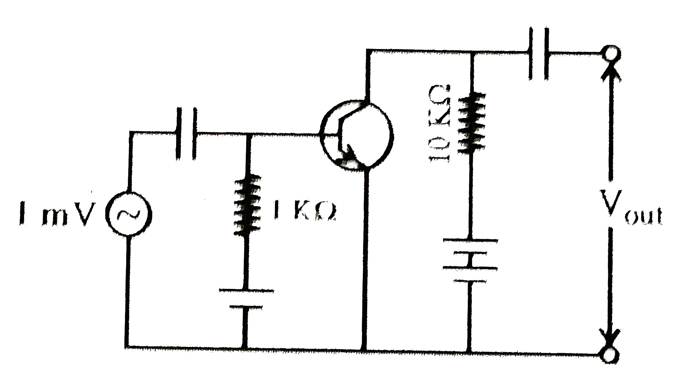
  5. The voltage gain of the following amplifier is

    Text Solution

    |

  6. For CE transistor amplifier, the audio signal voltage across the colle...

    Text Solution

    |

  7. In a p-n junction diode, change in temperature due to heating

    Text Solution

    |

  8. In the circuit shows in the figure, the input voltage V(i) is 20 V,...

    Text Solution

    |

  9. In a common emitter transistor amplifier the audio signal voltage acro...

    Text Solution

    |

  10. Boolean algebra is essentially based on

    Text Solution

    |

  11. The output of OR gate is 1

    Text Solution

    |

  12. The following figure shows a logic gate circuit with two inputs A and ...

    Text Solution

    |

  13. Which of the following logic gates is an universal gate?

    Text Solution

    |

  14. The output (X) of the logic circuit shown in figure will be

    Text Solution

    |

  15. To get an output 1 from the circuit shown in the figure, the input mus...

    Text Solution

    |

  16. The circuit is equivalent to

    Text Solution

    |

  17. What is the output Y in the following circuit, when all the three inpu...

    Text Solution

    |

  18. In the combination of the following gates the output Y can be written ...

    Text Solution

    |

  19. The given electrical network is equivalent to

    Text Solution

    |

  20. The correct boolean operation represented by the circuit diagram drawn...

    Text Solution

    |