A
B
C
D
Text Solution
Verified by Experts
The correct Answer is:


Topper's Solved these Questions
Similar Questions
Explore conceptually related problems
ERRORLESS-ELECTRONICS-Assertion & Reason
- Statement-1 : The temperature coefficient of resistance is positive fo...
Text Solution
|
- Assertion: Electron has higher mobility than hole in a semiconductor. ...
Text Solution
|
- Assertion : An N-type semiconductor has a large number of electrons bu...
Text Solution
|
- Assertion : Light emitting diode (LED) emits spontaneous radiation. ...
Text Solution
|
- Assertion: Silicon is preferred over germanium for making semiconducto...
Text Solution
|
- Assertion: We can measure the potential barrier of a PN junction by pu...
Text Solution
|
- Assertion : The energy gap between the valence band and conduction ban...
Text Solution
|
- Assertion: Two P-N junction diodes placed back to back, will work as a...
Text Solution
|
- Assertion : In transistor common emitter mode as an amplifier is pre...
Text Solution
|
- Assertion:The dominant mechanism for motion of charge carriers in forw...
Text Solution
|
- Statement-I : A p-n junction with reverse bias can be used as a photod...
Text Solution
|
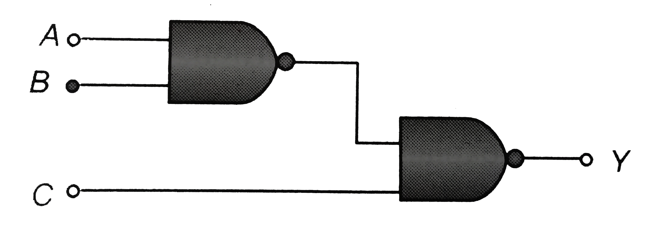
- Assertion: NAND or NOR gates are called digital building blocks. Rea...
Text Solution
|
- Assertion : In common base configuration, the current gain of the tran...
Text Solution
|
- Assertion : In the following circuit the potential drop across the res...
Text Solution
|
- Assertion: The current gain in common base circuit is always less than...
Text Solution
|
- Assertion: V-i charcteristic of P-N junction diode is same as that of ...
Text Solution
|
- Assertion: Zener diode works on a principle of of breakdown voltage. ...
Text Solution
|
- Assertion: NOT gate is also called inverter circuit. Reason: NOT gat...
Text Solution
|
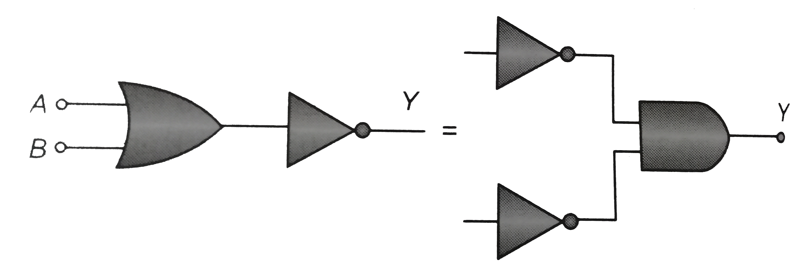
- Assertion: De Morgan's theoram bar(A+B)=bar(A).bar(B) may be explained...
Text Solution
|
- Assertion: A P-N photodiode is made from a semiconductor for which E(...
Text Solution
|