Text Solution
Verified by Experts


Topper's Solved these Questions
SEMICONDUCTOR ELECTRONICS: MATERIALS, DEVICES AND SIMPLE CIRCUITS
AAKASH INSTITUTE|Exercise Try yourself|20 VideosSEMICONDUCTOR ELECTRONICS: MATERIALS, DEVICES AND SIMPLE CIRCUITS
AAKASH INSTITUTE|Exercise Assignment (Section -A (Objective Type question (One option is correct))|50 VideosSEMICONDUCTOR ELECTRONICS (MATERIAL, DEVICES AND SIMPLE CIRUITS )
AAKASH INSTITUTE|Exercise Assignment SECTION - D (Assertion & reason type Question)|10 VideosSYSTEM OF PARTICLES AND ROTATIONAL MOTION
AAKASH INSTITUTE|Exercise Try Yourself|63 Videos
Similar Questions
Explore conceptually related problems
AAKASH INSTITUTE-SEMICONDUCTOR ELECTRONICS: MATERIALS, DEVICES AND SIMPLE CIRCUITS-Assignment (Section-D (Assertion and reason))
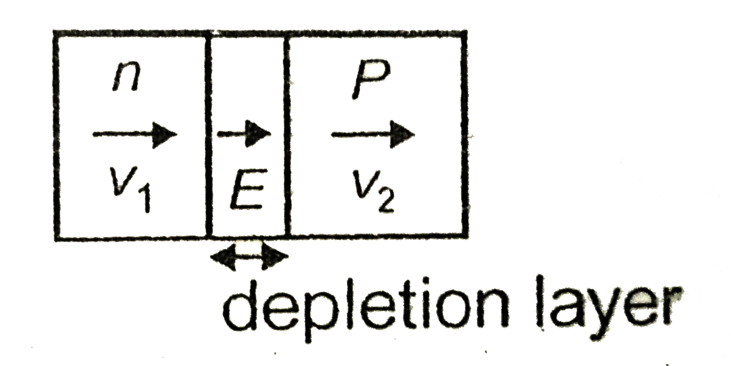
- In a p-n junction, the thickness of depletion region is 2xx10^(-7)m an...
Text Solution
|
- Assertion:To make p type semiconductor , pentavalent impurity like pho...
Text Solution
|
- Assertion: In forward biasing current starts when minimum voltage of b...
Text Solution
|
- Assertion: LED is used in display units because it emits light when cu...
Text Solution
|
- Assertion: In reverse biased condition a p-n junction diode does not c...
Text Solution
|
- Assertion: A transistor can be used as an amplifier. Reason: A small...
Text Solution
|