Text Solution
Verified by Experts


Topper's Solved these Questions
SEMICONDUCTOR ELECTRONICS: MATERIALS, DEVICES AND SIMPLE CIRCUITS
AAKASH INSTITUTE|Exercise Assignment (Section -A (Objective Type question (One option is correct))|50 VideosSEMICONDUCTOR ELECTRONICS: MATERIALS, DEVICES AND SIMPLE CIRCUITS
AAKASH INSTITUTE|Exercise Assignment (Section -B (Objective type question (one option is correct))|29 VideosSEMICONDUCTOR ELECTRONICS: MATERIALS, DEVICES AND SIMPLE CIRCUITS
AAKASH INSTITUTE|Exercise Assignment (Section-D (Assertion and reason))|5 VideosSEMICONDUCTOR ELECTRONICS (MATERIAL, DEVICES AND SIMPLE CIRUITS )
AAKASH INSTITUTE|Exercise Assignment SECTION - D (Assertion & reason type Question)|10 VideosSYSTEM OF PARTICLES AND ROTATIONAL MOTION
AAKASH INSTITUTE|Exercise Try Yourself|63 Videos
Similar Questions
Explore conceptually related problems
AAKASH INSTITUTE-SEMICONDUCTOR ELECTRONICS: MATERIALS, DEVICES AND SIMPLE CIRCUITS-Try yourself
- In semiconductor at a room temperature
Text Solution
|
- Carbon, silicon and germanium atoms have four valence electrons each. ...
Text Solution
|
- In a pure semiconductor, the number of conduction electron is 6xx10^(1...
Text Solution
|
- C, Si and Ge have same lattice structure. Why is C insulator, while ...
Text Solution
|
- A semiconductor is known to have an electron concentration of 6xx10^(1...
Text Solution
|
- Suppose a pure Si-crystal has 5xx10^(28) "atoms" m^(-3). It is doped b...
Text Solution
|
- What is the current through an ideal p-n junction diode shown in figur...
Text Solution
|
- Which of the following diodes is forward-biased ?
Text Solution
|
- Can we take one slab of p - type semiconductor and physically join i...
Text Solution
|
- The V-I characteristic of a silicon diode is shown in the figure. Calc...
Text Solution
|
- Freuency of given AC signal is 50 Hz. When it connected to a half - wa...
Text Solution
|
- What is the output form of full-wave rectifier ?
Text Solution
|
- In a zener-regulated power supply a zener diode with V(Z)=6 volt is u...
Text Solution
|
- The current in the forward bias is unknown to be more (~mA) than the c...
Text Solution
|
- Why are Si and GaAs are preferred materials for solar cells?
Text Solution
|
- For a CE transistor amplifier, the audio signal voltage across the col...
Text Solution
|
- In common emitter transistor as shown in Fig., the V(BB) supply can be...
Text Solution
|
- Show the output waveform of OR gate for the following input waveforms ...
Text Solution
|
- Sketch the output waveform obtained from AND gate for the following in...
Text Solution
|
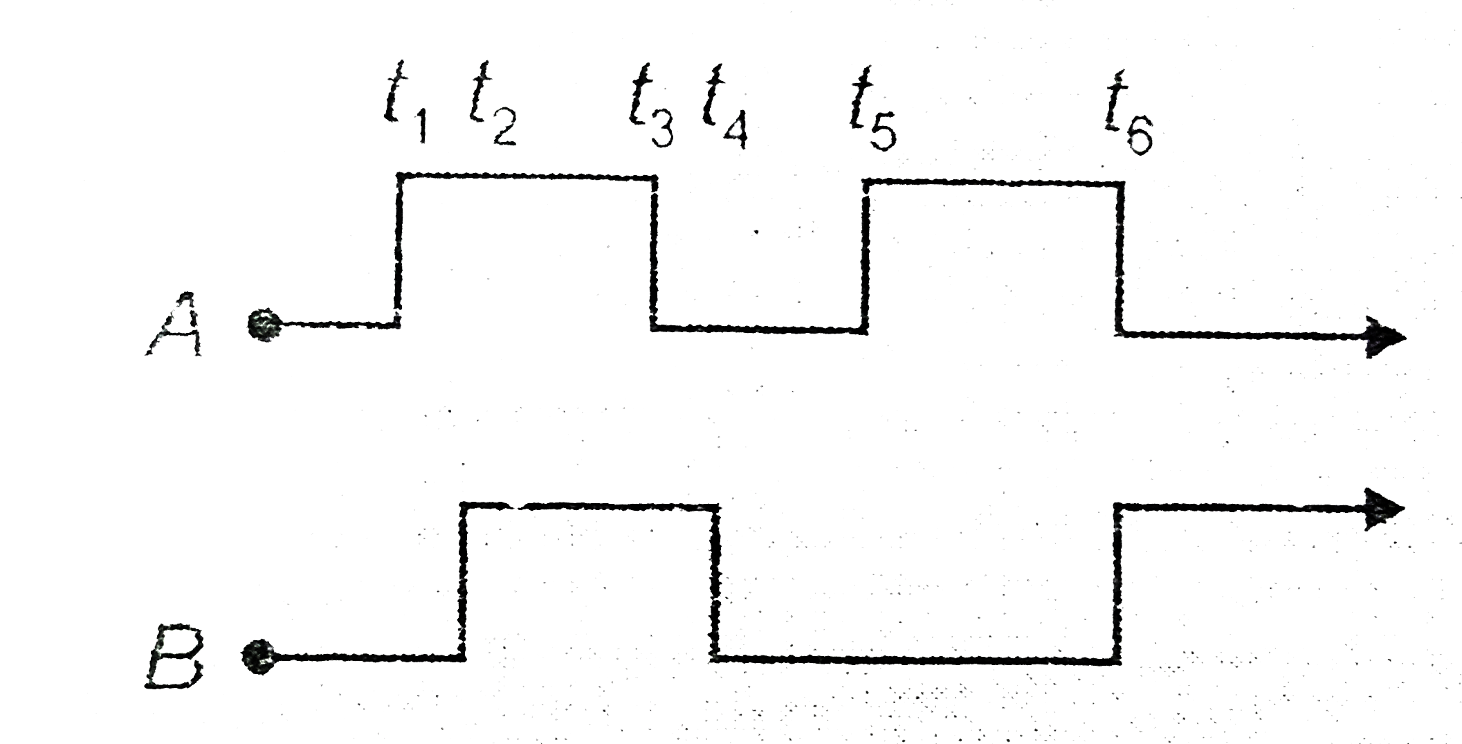
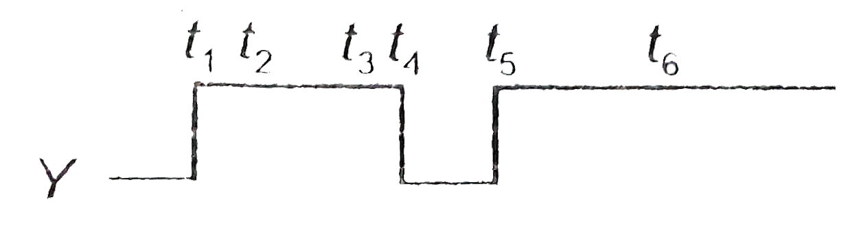
- Sketch the output wavefrom Y from a NAND gate having following inputs ...
Text Solution
|