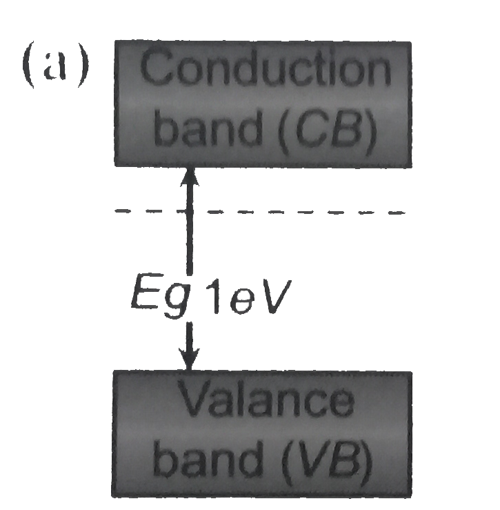
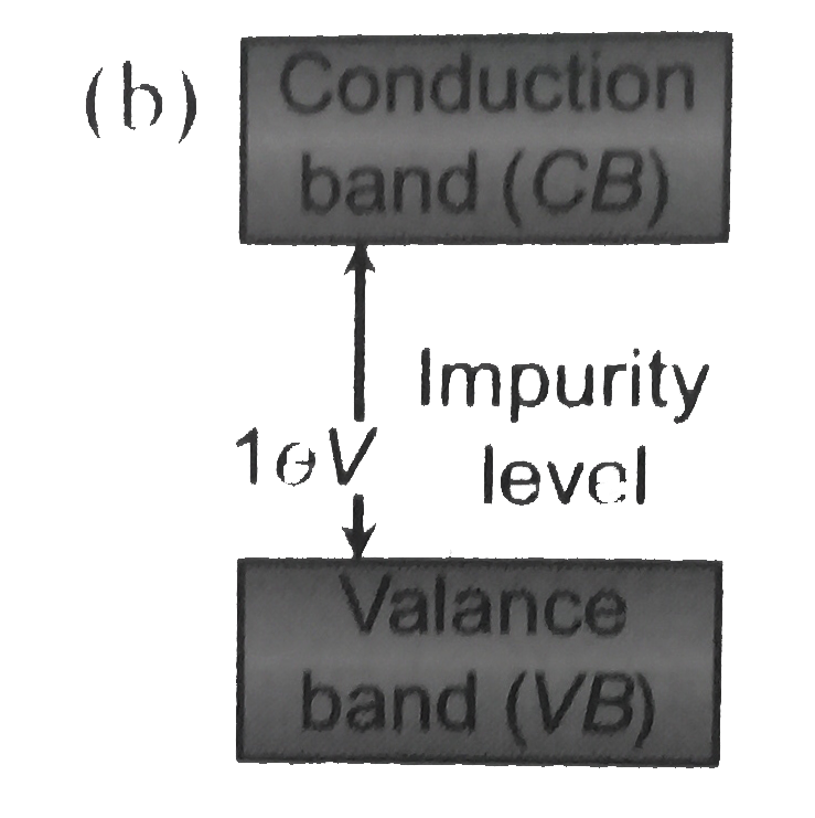
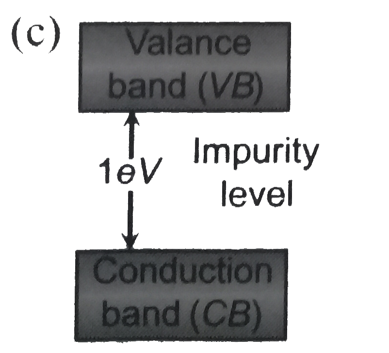
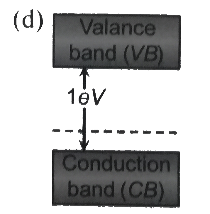
Home
Class 12
PHYSICS
Which of the following energy band diagr...

Which of the following energy band diagrams shows the `N`-type semiconductor?

A

B

C

D

Text Solution

AI Generated Solution

The correct Answer is:
To determine which energy band diagram represents an N-type semiconductor, we need to understand the characteristics of N-type semiconductors and how they are depicted in energy band diagrams. Here’s a step-by-step solution: ### Step 1: Understand the Structure of Energy Bands In semiconductors, there are two main energy bands: the valence band and the conduction band. The valence band is filled with electrons, while the conduction band is where electrons can move freely and conduct electricity. **Hint:** Remember that the conduction band is always above the valence band in energy diagrams. ### Step 2: Identify the Donor Level In N-type semiconductors, impurities (donors) are added to the semiconductor material. These donor atoms have extra electrons that can be easily excited into the conduction band. The energy level of these donor electrons is typically just below the conduction band. **Hint:** Look for a level close to the conduction band that represents the donor electrons. ### Step 3: Analyze the Given Options We have four options (A, B, C, D). We need to check each one for the following: - The conduction band should be above the valence band. - There should be a donor level present, which is close to the conduction band. **Hint:** Disregard any options where the conduction band is below the valence band, as they cannot represent an N-type semiconductor. ### Step 4: Evaluate Each Option - **Options C and D:** Both have the valence band above the conduction band, which is incorrect for any semiconductor, including N-type. - **Options A and B:** Both have the correct order of bands (conduction band above valence band). However, only option A shows a defined donor level near the conduction band. **Hint:** Focus on the presence of the donor level in options A and B. ### Step 5: Conclusion Since option A is the only one that shows the donor level near the conduction band, it is the correct representation of an N-type semiconductor. **Final Answer:** Option A is the correct energy band diagram for an N-type semiconductor.

To determine which energy band diagram represents an N-type semiconductor, we need to understand the characteristics of N-type semiconductors and how they are depicted in energy band diagrams. Here’s a step-by-step solution: ### Step 1: Understand the Structure of Energy Bands In semiconductors, there are two main energy bands: the valence band and the conduction band. The valence band is filled with electrons, while the conduction band is where electrons can move freely and conduct electricity. **Hint:** Remember that the conduction band is always above the valence band in energy diagrams. ### Step 2: Identify the Donor Level ...
Promotional Banner

Topper's Solved these Questions

  • SEMICONDUCTOR ELECTRONICS

    A2Z|Exercise Junction Diode|57 Videos
  • SEMICONDUCTOR ELECTRONICS

    A2Z|Exercise Diode In Circuits|40 Videos
  • SEMICONDUCTOR ELECTRONICS

    A2Z|Exercise EXERCISE|29 Videos
  • NUCLEAR PHYSICS

    A2Z|Exercise Section D - Chapter End Test|29 Videos
  • SOURCE AND EFFECT OF MAGNETIC FIELD

    A2Z|Exercise Section D - Chapter End Test|30 Videos

Similar Questions

Explore conceptually related problems

n-type semiconductor is

A N -type semiconductor is

A N - type semiconductor is

An n-type semiconductor is

What are n-type semiconductors ?

Show the acceptor energy level in energy band diagram of p-type semiconductor.

A2Z-SEMICONDUCTOR ELECTRONICS-Classification Of Metals
  1. In P-type semiconductor, there is

    Text Solution

    |

  2. The velence of the impurity atom that is to the be added to garmenium ...

    Text Solution

    |

  3. Which of the following energy band diagrams shows the N-type semicondu...

    Text Solution

    |

  4. If n(e) and n(h) be the number of electrons and drift velocity in a se...

    Text Solution

    |

  5. The energy gap of silicon is 1.14 eV. The maximum wavelength at which ...

    Text Solution

    |

  6. A Ge specimen is doped with Al. The concentration of acceptor atoms is...

    Text Solution

    |

  7. The electron mobility in N-type germanium is 3900cm^(2)//v-s and its c...

    Text Solution

    |

  8. In a semiconducting material the mobilities of electrons and holes are...

    Text Solution

    |

  9. Which of the energy band diagrams shown in the figure corresponds to t...

    Text Solution

    |

  10. The energy band diagrams for three semiconductor samples of silicon ar...

    Text Solution

    |

  11. Carbon , silicon and germanium have four valence elcectrons each . The...

    Text Solution

    |

  12. when the electrical conductivity of a semiconductor is due to the brea...

    Text Solution

    |

  13. If N(P) and N(e) be the numbers of holes and conduction electrons in a...

    Text Solution

    |

  14. In intrinsic semiconductor at room of current carriers would be

    Text Solution

    |

  15. Intrinsic semiconductor is electrically neutral. Extrinsic semiconduct...

    Text Solution

    |

  16. In extrinsic semiconductors

    Text Solution

    |

  17. The width of forbidden gap in silicon crystal is 1.1 eV. When the crys...

    Text Solution

    |

  18. A silicon specimen is made into a P-type semiconductor by dopping, on ...

    Text Solution

    |

  19. In a pure silicon (n(i)=10^(16)//m^(3)) crystal at 300K, 10^(21) atoms...

    Text Solution

    |

  20. A PN junction diode cannot be used

    Text Solution

    |