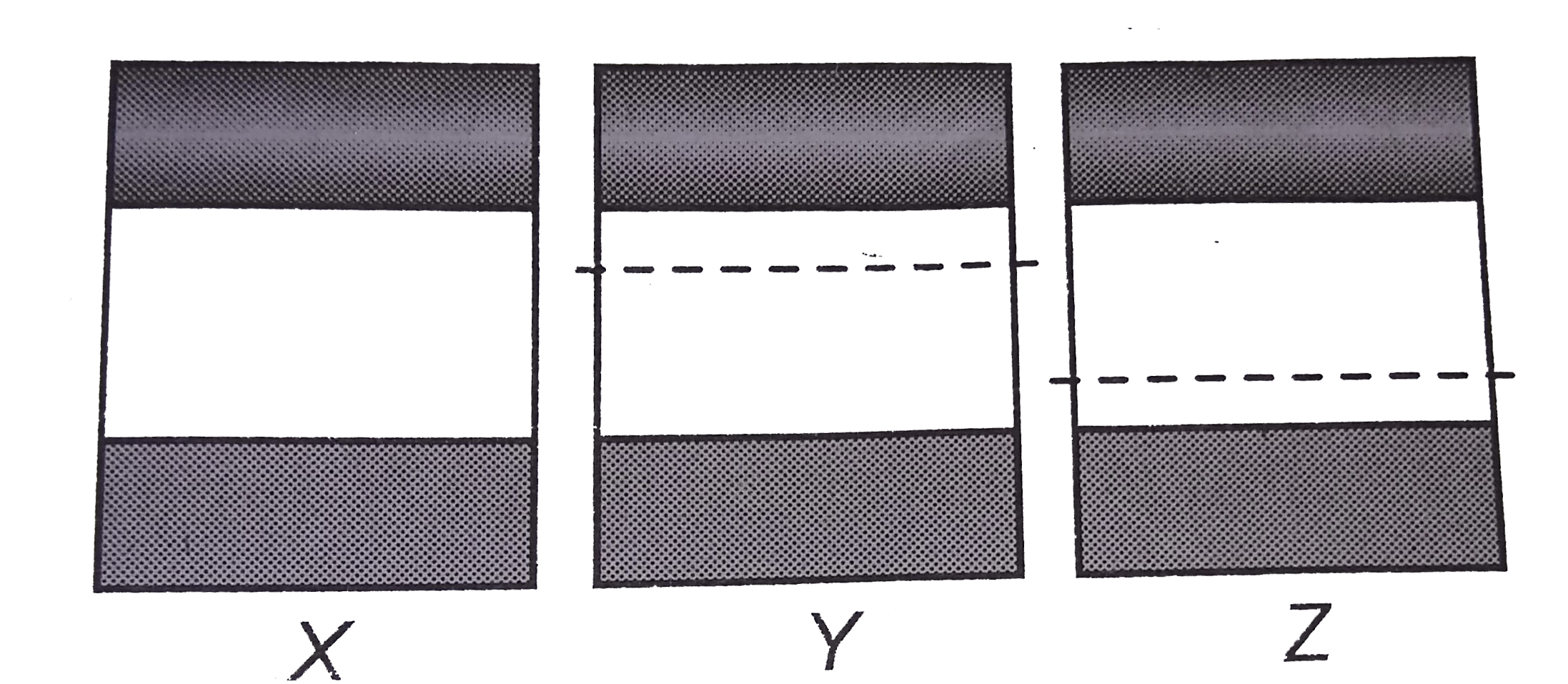
A
B
C
D
Text Solution
Verified by Experts
The correct Answer is:
Topper's Solved these Questions
SEMICONDUCTOR ELECTRONICS
A2Z|Exercise Junction Diode|57 VideosSEMICONDUCTOR ELECTRONICS
A2Z|Exercise Diode In Circuits|40 VideosSEMICONDUCTOR ELECTRONICS
A2Z|Exercise EXERCISE|29 VideosNUCLEAR PHYSICS
A2Z|Exercise Section D - Chapter End Test|29 VideosSOURCE AND EFFECT OF MAGNETIC FIELD
A2Z|Exercise Section D - Chapter End Test|30 Videos
Similar Questions
Explore conceptually related problems
A2Z-SEMICONDUCTOR ELECTRONICS-Classification Of Metals
- In P-type semiconductor, there is
Text Solution
|
- The velence of the impurity atom that is to the be added to garmenium ...
Text Solution
|
- Which of the following energy band diagrams shows the N-type semicondu...
Text Solution
|
- If n(e) and n(h) be the number of electrons and drift velocity in a se...
Text Solution
|
- The energy gap of silicon is 1.14 eV. The maximum wavelength at which ...
Text Solution
|
- A Ge specimen is doped with Al. The concentration of acceptor atoms is...
Text Solution
|
- The electron mobility in N-type germanium is 3900cm^(2)//v-s and its c...
Text Solution
|
- In a semiconducting material the mobilities of electrons and holes are...
Text Solution
|
- Which of the energy band diagrams shown in the figure corresponds to t...
Text Solution
|
- The energy band diagrams for three semiconductor samples of silicon ar...
Text Solution
|
- Carbon , silicon and germanium have four valence elcectrons each . The...
Text Solution
|
- when the electrical conductivity of a semiconductor is due to the brea...
Text Solution
|
- If N(P) and N(e) be the numbers of holes and conduction electrons in a...
Text Solution
|
- In intrinsic semiconductor at room of current carriers would be
Text Solution
|
- Intrinsic semiconductor is electrically neutral. Extrinsic semiconduct...
Text Solution
|
- In extrinsic semiconductors
Text Solution
|
- The width of forbidden gap in silicon crystal is 1.1 eV. When the crys...
Text Solution
|
- A silicon specimen is made into a P-type semiconductor by dopping, on ...
Text Solution
|
- In a pure silicon (n(i)=10^(16)//m^(3)) crystal at 300K, 10^(21) atoms...
Text Solution
|
- A PN junction diode cannot be used
Text Solution
|
