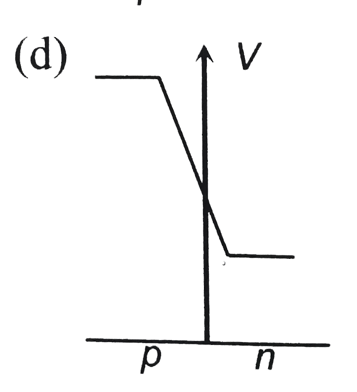
A
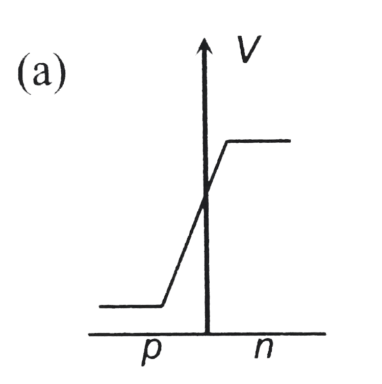
B
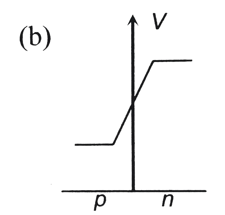
C
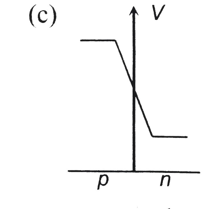
D
Text Solution
Verified by Experts
The correct Answer is:


Topper's Solved these Questions
SEMICONDUCTOR ELECTRONICS
A2Z|Exercise Diode In Circuits|40 VideosSEMICONDUCTOR ELECTRONICS
A2Z|Exercise Junction Transistor|47 VideosSEMICONDUCTOR ELECTRONICS
A2Z|Exercise Classification Of Metals|64 VideosNUCLEAR PHYSICS
A2Z|Exercise Section D - Chapter End Test|29 VideosSOURCE AND EFFECT OF MAGNETIC FIELD
A2Z|Exercise Section D - Chapter End Test|30 Videos
Similar Questions
Explore conceptually related problems
A2Z-SEMICONDUCTOR ELECTRONICS-Junction Diode
- A device in which P and N-type semiconductors are used is more useful ...
Text Solution
|
- The depletion layer in diode is 1 mum wide and the knee potential is 0...
Text Solution
|
- If a full wave reactifier circuit is operating from 50 Hz mains, the f...
Text Solution
|
- In a p- n junction diode not connected to any circuit,
Text Solution
|
- Which of the following statement is not true ?
Text Solution
|
- The dominant mechanisms for motion of charge carriers in forward and r...
Text Solution
|
- In P-N junction, avalanche current flows in circuit when biassing is
Text Solution
|
- The depletion layer in P-N junction region is caused by
Text Solution
|
- The reason of current flow in P-N junction forward biase is
Text Solution
|
- The resistance of a revese biased P-N junction diode is about
Text Solution
|
- No biase is applied to a P-N junction, then the current
Text Solution
|
- Zener diode is used as
Text Solution
|
- In P-N junction, the barrier potential offerse resistance to
Text Solution
|
- A semiconducting device is connected in a series circuit with a batter...
Text Solution
|
- The approximate ratio of resistance in the forward and reverse biase o...
Text Solution
|
- In a forward biased PN- junction diode, the potential barrier in the d...
Text Solution
|
- Different voltages are applied across a P-N junction and the currents ...
Text Solution
|
- Consider the following statement A and B and identify the correct choi...
Text Solution
|
- A P-type semiconductor has acceptor levels 57 meV above the valence ba...
Text Solution
|
- Which one is forward biase?
Text Solution
|