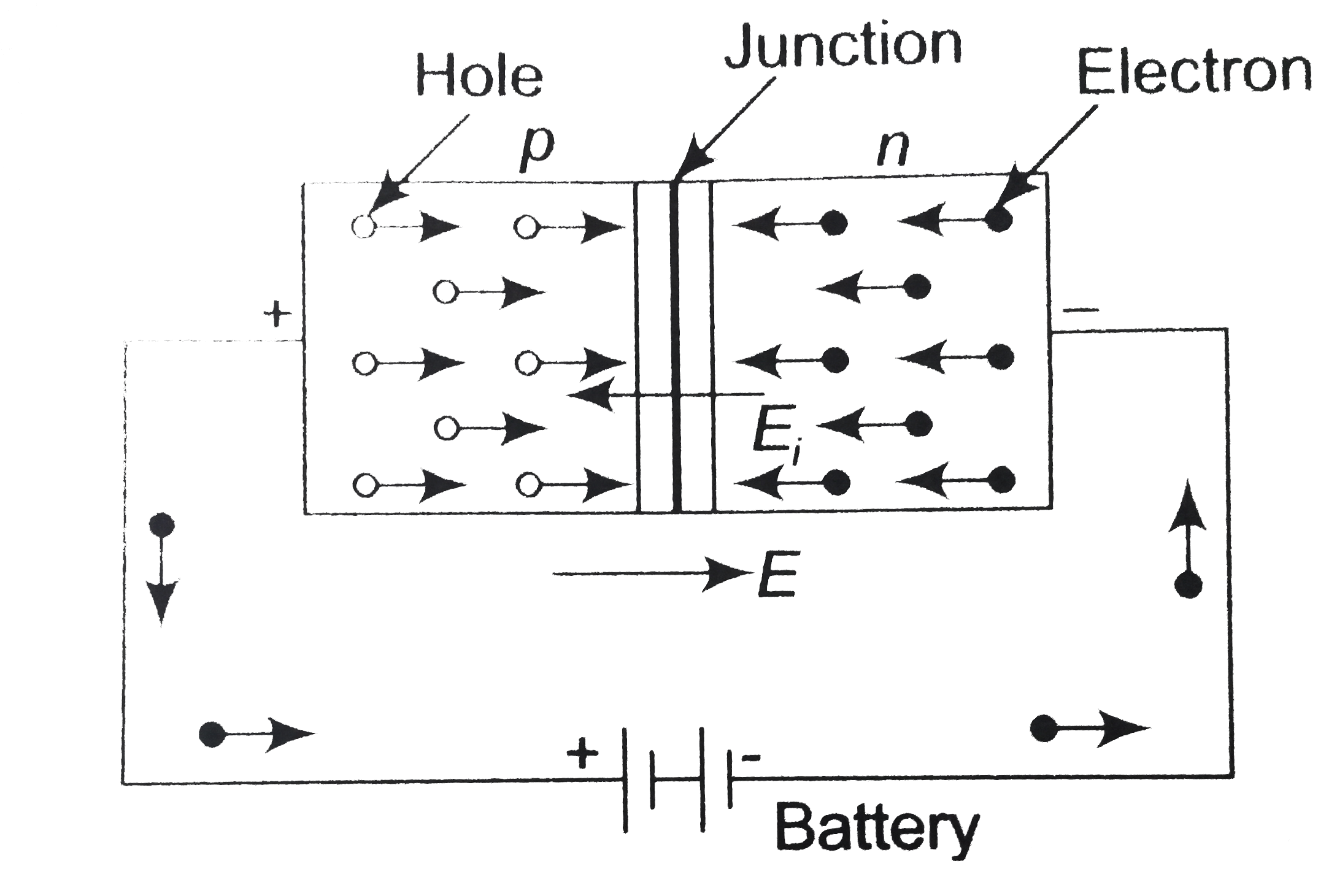
A
B
C
D
Text Solution
Verified by Experts
The correct Answer is:
Topper's Solved these Questions
SEMICONDUCTOR ELECTRONICS
A2Z|Exercise AIIMS Questions|38 VideosSEMICONDUCTOR ELECTRONICS
A2Z|Exercise Assertion Reason|18 VideosSEMICONDUCTOR ELECTRONICS
A2Z|Exercise Section B - Assertion Reasoning|22 VideosNUCLEAR PHYSICS
A2Z|Exercise Section D - Chapter End Test|29 VideosSOURCE AND EFFECT OF MAGNETIC FIELD
A2Z|Exercise Section D - Chapter End Test|30 Videos
Similar Questions
Explore conceptually related problems
A2Z-SEMICONDUCTOR ELECTRONICS-AIPMT/NEET Questions
- Choose the only false statement form the following
Text Solution
|
- Carbon , silicon and germanium have four valence elcectrons each . The...
Text Solution
|
- Application of a forward biase to a p-n junction:
Text Solution
|
- Zenor diode is used for
Text Solution
|
- Copper has face centred cubic (fc c) lattice with interatomic spacing ...
Text Solution
|
- The following figure shows a logic gate circuit with two inputs A and ...
Text Solution
|
- A transistor is operated in common emitter configuration at constant c...
Text Solution
|
- A forward biased diode is
Text Solution
|
- The radius of germanium (Ge) nuclide is measured to be twice the radiu...
Text Solution
|
- In the following circuit, the output Y for all possible inputs A and B...
Text Solution
|
- A common emitter amplifier has a voltage gain of 50, an input impedenc...
Text Solution
|
- For a cubic crystal structure which one of the following relations ind...
Text Solution
|
- In the energy band diagram of a material shown below, the open circles...
Text Solution
|
- The voltage gain of an amplifier with 9% negative feedback is 10. The ...
Text Solution
|
- A p-n photodiode is made of a material with a band gap of 2.0 eV. The ...
Text Solution
|
- The circuit is equivalent to
Text Solution
|
- A p-n photodiode is fabricated from a semiconductor with a band gap of...
Text Solution
|
- A transistor is operated in common emitter configuration at V(c)=2 V s...
Text Solution
|
- The number of beta particles emitter by radioactive sustance is twice ...
Text Solution
|
- Sodium has body centred packing. Distance between two nearest atoms is...
Text Solution
|
