Home
Class 12
PHYSICS
In the energy band diagram of a material...

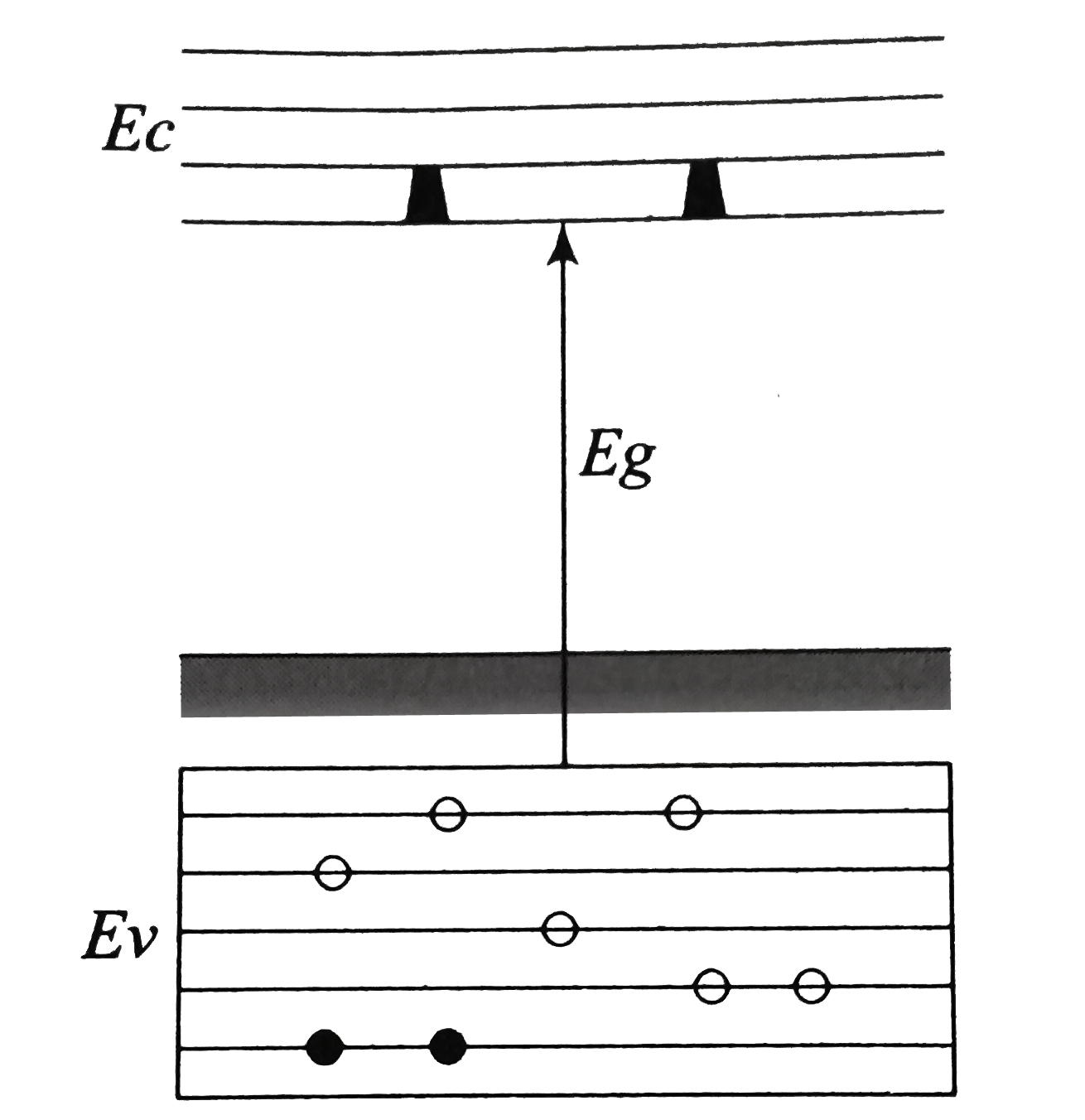
In the energy band diagram of a material shown below, the open circles and filled circles denote holes and electrons respectively. The material is a/an

A

`p`-type semiconductor

B

insulator

C

metal

D

`n` type semiconductor

Text Solution

Verified by Experts

The correct Answer is:
A

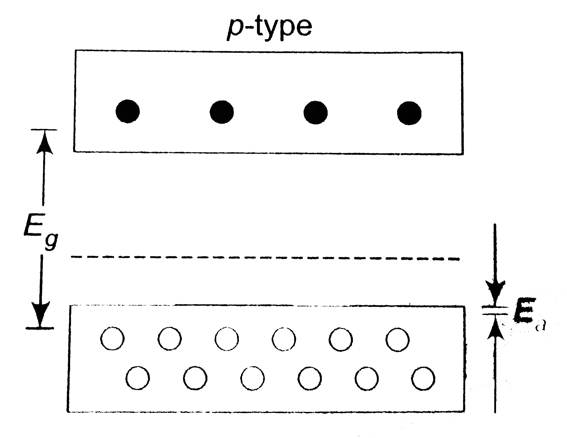
The given figure represents `p`-type semiconductor as described below
When one of the silicon atom (valence =`4`) has been replaced by an atom of aluminium (valence `=3`), the aluminium atom can bond covalently with only three aluminium atom can bond covalently with only three silicon atoms, so there is now a "missing" electron (a hole) in one alumiumium-silicon bond with a small expendicture of energy, an electron can be torn from a neigbouring silicon-silicon bond to fill this hole, thereby creating a hole in that bond. similarly, an electron from some other bond can be moved to fill the second hole. In this way, the hole can migrate through the lattice.

The alumunium atom is called an acceptor atom because it readily accetps an electron from a neighbouring bond that is from the valence band of silicon. As figure suggests, this electron occupies a localized acceptor satate that lies within the energy gap, at an average energy interval `E_(a)` above the top of the valence band. By adding acceptor atoms, it is possible to increase very greately the number of holes in the valence band.
Promotional Banner

Topper's Solved these Questions

  • SEMICONDUCTOR ELECTRONICS

    A2Z|Exercise AIIMS Questions|38 Videos
  • SEMICONDUCTOR ELECTRONICS

    A2Z|Exercise Assertion Reason|18 Videos
  • SEMICONDUCTOR ELECTRONICS

    A2Z|Exercise Section B - Assertion Reasoning|22 Videos
  • NUCLEAR PHYSICS

    A2Z|Exercise Section D - Chapter End Test|29 Videos
  • SOURCE AND EFFECT OF MAGNETIC FIELD

    A2Z|Exercise Section D - Chapter End Test|30 Videos

Similar Questions

Explore conceptually related problems

In the circuit diagram shown below , the magnitude and direction of the flow of current , respectively , would be

Which of the energy band diagrams shown in the figure corresponds to that of a semiconductor?

Assertion: If there is some gap between the conduction band and the valence band, electrons in the valence band all remain bound and no free electrons are available in the conduction band. Then the material is an insulator. Reason: Resistance of insulators is very low

If p is the resistivity of a material, and n is the number density of free electrons in it, the mean time between collisions between electrons in the material is given by: (m denotes the mass of an electron, and e denotes the charge on an electron)

Draw the "energy bands" diagram for a (i) pure semiconductor (ii) insulator. How does the energy band, foe a pure semiconductor, get affected when this semiconductor is doped with an acceptor impurity donor impurity? Hence discuss why the 'holes' and the 'electrons' respectively, become the 'majority charge carriers' in these two cases.

For the circle shown below, find the length. (in cm) of the largest cord of the circle.

Study the following diagram consisting of a circle, a rectangle and a triangle and answer the question given below it. If the circle is called 'rectangle rectangle is called triangle' and triangle is called 'circle', which number is only in the triangle but not in other two diagrams?

The energy band diagrams for three semiconductor samples of silicon are as shown. We can then assert that

A2Z-SEMICONDUCTOR ELECTRONICS-AIPMT/NEET Questions
  1. A common emitter amplifier has a voltage gain of 50, an input impedenc...

    Text Solution

    |

  2. For a cubic crystal structure which one of the following relations ind...

    Text Solution

    |

  3. In the energy band diagram of a material shown below, the open circles...

    Text Solution

    |

  4. The voltage gain of an amplifier with 9% negative feedback is 10. The ...

    Text Solution

    |

  5. A p-n photodiode is made of a material with a band gap of 2.0 eV. The ...

    Text Solution

    |

  6. The circuit is equivalent to

    Text Solution

    |

  7. A p-n photodiode is fabricated from a semiconductor with a band gap of...

    Text Solution

    |

  8. A transistor is operated in common emitter configuration at V(c)=2 V s...

    Text Solution

    |

  9. The number of beta particles emitter by radioactive sustance is twice ...

    Text Solution

    |

  10. Sodium has body centred packing. Distance between two nearest atoms is...

    Text Solution

    |

  11. Which one of the following statement is false?

    Text Solution

    |

  12. Which one of the following bonds produces a solid taht reflects light ...

    Text Solution

    |

  13. The device that can act as a complete electronic circuit is

    Text Solution

    |

  14. In order to obtain an output Y=1 form the circuit of fig. the inputs m...

    Text Solution

    |

  15. A transistor is operated in common emitter configuration at V(c)=2 V s...

    Text Solution

    |

  16. In forward bias, the width of potential barrier in a P-N junction diod...

    Text Solution

    |

  17. Symbolic representation of four logic gates are shown as

    Text Solution

    |

  18. If a small amount of antimony is added to germanium crystal

    Text Solution

    |

  19. In the following figure, the diodes, which are forward biased, are

    Text Solution

    |

  20. Pure Si at 500K has equal number of electron (n(e)) and hole (n(h)) co...

    Text Solution

    |