A
B
C
D
Text Solution
Verified by Experts
The correct Answer is:


Topper's Solved these Questions
SEMICONDUCTOR ELECTRONICS
A2Z|Exercise AIIMS Questions|38 VideosSEMICONDUCTOR ELECTRONICS
A2Z|Exercise Assertion Reason|18 VideosSEMICONDUCTOR ELECTRONICS
A2Z|Exercise Section B - Assertion Reasoning|22 VideosNUCLEAR PHYSICS
A2Z|Exercise Section D - Chapter End Test|29 VideosSOURCE AND EFFECT OF MAGNETIC FIELD
A2Z|Exercise Section D - Chapter End Test|30 Videos
Similar Questions
Explore conceptually related problems
A2Z-SEMICONDUCTOR ELECTRONICS-AIPMT/NEET Questions
- Which one of the following bonds produces a solid taht reflects light ...
Text Solution
|
- The device that can act as a complete electronic circuit is
Text Solution
|
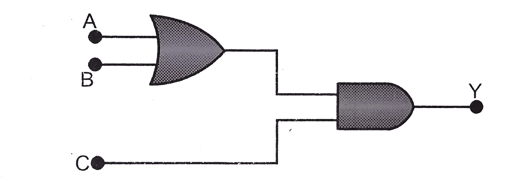
- In order to obtain an output Y=1 form the circuit of fig. the inputs m...
Text Solution
|
- A transistor is operated in common emitter configuration at V(c)=2 V s...
Text Solution
|
- In forward bias, the width of potential barrier in a P-N junction diod...
Text Solution
|
- Symbolic representation of four logic gates are shown as
Text Solution
|
- If a small amount of antimony is added to germanium crystal
Text Solution
|
- In the following figure, the diodes, which are forward biased, are
Text Solution
|
- Pure Si at 500K has equal number of electron (n(e)) and hole (n(h)) co...
Text Solution
|
- A zener diode, having breakdown voltage equal to 15 V is used in a vol...
Text Solution
|
- Two ideal diodes are connected to a battery as shown in the circuit. T...
Text Solution
|
- In a CE transistor amplifier, the audio signal voltage across the coll...
Text Solution
|
- C and Si both have same lattice structure, having 4 bonding electrons ...
Text Solution
|
- Transfer characterstics [output voltage (V(o)) vs. input voltage (V(i)...
Text Solution
|
- The figure shows a logic circuit with two inputs A and B and the outpu...
Text Solution
|
- The input resistance of a silicon transistor is 100 Omega. Base curren...
Text Solution
|
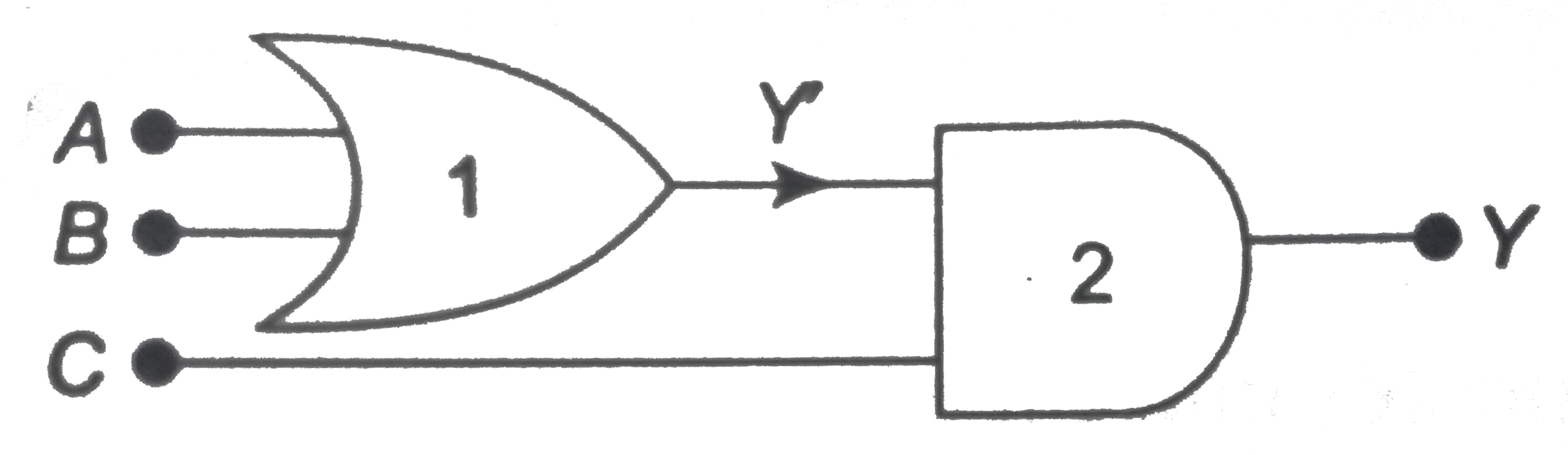
- In order to obtain an output Y=1 form the circuit of fig. the inputs m...
Text Solution
|
- In a n-type semiconductor, which of the following statement is true?
Text Solution
|
- In a common emitter (CE) amplifier having a voltage gain G, the transi...
Text Solution
|
- The output (X) of the logic circuit shown in figure will be
Text Solution
|