
A
B
C
D
Text Solution
Verified by Experts
The correct Answer is:


Topper's Solved these Questions
SEMICONDUCTOR ELECTRONICS
A2Z|Exercise Assertion Reason|18 VideosSEMICONDUCTOR ELECTRONICS
A2Z|Exercise SECTION -D|1 VideosSEMICONDUCTOR ELECTRONICS
A2Z|Exercise AIPMT/NEET Questions|77 VideosNUCLEAR PHYSICS
A2Z|Exercise Section D - Chapter End Test|29 VideosSOURCE AND EFFECT OF MAGNETIC FIELD
A2Z|Exercise Section D - Chapter End Test|30 Videos
Similar Questions
Explore conceptually related problems
A2Z-SEMICONDUCTOR ELECTRONICS-AIIMS Questions
- For sky wave propagation of 10 MHz signal, what should be the minimum ...
Text Solution
|
- Reverse bias applied to a junction diode
Text Solution
|
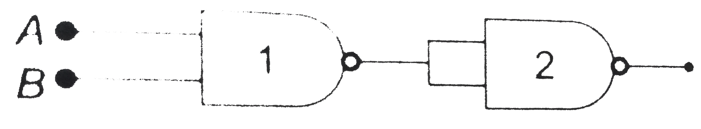
- The circuit given below represents which of the logic operations?
Text Solution
|
- An amplifier has a voltage gain A(V)=1000. The voltage gain in dB is
Text Solution
|
- A light emitting diode (LED) has a voltage drop of 2V across it and pa...
Text Solution
|
- The minimum potential difference between the base and emitter required...
Text Solution
|
- If in a p-n junction diode , a square input single of 10 V is applied...
Text Solution
|
- The input resistance of a common emitter transistor amplifer, if the o...
Text Solution
|
- The combination of the gates shown in the figure below produces
Text Solution
|
- In case of NPN-transistor the collector current is always less than th...
Text Solution
|
- The following truth table corresponds to the logic gate |(A,0,0,1,1)...
Text Solution
|
- In transistor, a change of 8.0 mA in the emitter current produces a ch...
Text Solution
|
- A truth table is given below. Which of the following has this types fo...
Text Solution
|
- A semiconductor X is made by dopping a germanium crystal with arsenic ...
Text Solution
|
- The diode shown in the circuit is a silicon diode. The potential diffe...
Text Solution
|
- In the given figure, which of the diodes are forward biased?
Text Solution
|
- In a p- n junction diode not connected to any circuit,
Text Solution
|
- What will be the input of A and B for the Boolean expression bar((A+B)...
Text Solution
|
- The combination of 'NAND' gates shown here under (figure) are equivale...
Text Solution
|
- Find V(AB)
Text Solution
|