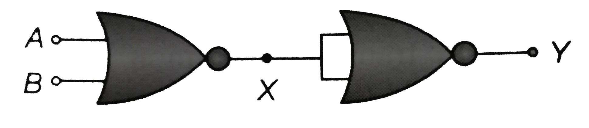
A
B
C
D
Text Solution
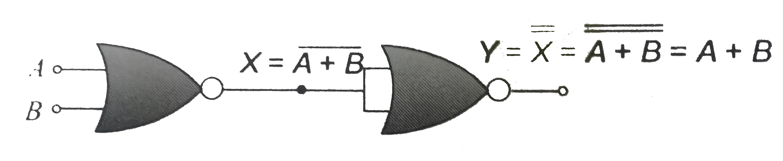
Verified by Experts
The correct Answer is:


Topper's Solved these Questions
SEMICONDUCTOR ELECTRONICS
A2Z|Exercise SECTION -D|1 VideosSEMICONDUCTOR ELECTRONICS
A2Z|Exercise EXERCISE|29 VideosSEMICONDUCTOR ELECTRONICS
A2Z|Exercise AIIMS Questions|38 VideosNUCLEAR PHYSICS
A2Z|Exercise Section D - Chapter End Test|29 VideosSOURCE AND EFFECT OF MAGNETIC FIELD
A2Z|Exercise Section D - Chapter End Test|30 Videos
Similar Questions
Explore conceptually related problems
A2Z-SEMICONDUCTOR ELECTRONICS-Assertion Reason
- Assertion: Microwave communication is preferred power optical communic...
Text Solution
|
- Assertion: The resistivity of a semiconductor increases with temperatu...
Text Solution
|
- Assertion: In a transistor the base is made thin. Reason: A thin bas...
Text Solution
|
- Assertion: A transistor amplifier is common emitter configuration has ...
Text Solution
|
- Assertion: Diode lasers are used as optical sources in optical communi...
Text Solution
|
- Assertion: The logic gate NOT can be built using diode. Reason: The ...
Text Solution
|
- Assertion: The number of electrons in a p-type silicon semiconductor i...
Text Solution
|
- Assertion: Television signals are recieved throgh sky-wave propagation...
Text Solution
|
- Assertion: Em wave with frequencies more than the critical frequency o...
Text Solution
|
- Assertion: In common base configuration, the current gain of the trans...
Text Solution
|
- Assertion: A p-n junction with reverse biase can be used as a photo-di...
Text Solution
|
- Assertion : The value of current through P - n junction in the given f...
Text Solution
|
- Assertion:The dominant mechanism for motion of charge carriers in forw...
Text Solution
|
- Assertion: The current gain in common base circuit is always less than...
Text Solution
|
- Assertion: NOT gate is also called inverter circuit. Reason: NOT gat...
Text Solution
|
- Assertion: In the following circuit the potential drop across the resi...
Text Solution
|
- Assertion: The following circuit represents 'OR' gate Reason: For...
Text Solution
|
- Assertion : An N-type semiconductor has a large number of electrons bu...
Text Solution
|