A
B
C
D
Text Solution
Verified by Experts
The correct Answer is:


Topper's Solved these Questions
Similar Questions
Explore conceptually related problems
A2Z-SEMICONDUCTOR ELECTRONICS-EXERCISE
- To obtain a P-type Si semiconductor, we need to dope pure Si with
Text Solution
|
- Two PN-junction can be connected in series by three different methods ...
Text Solution
|
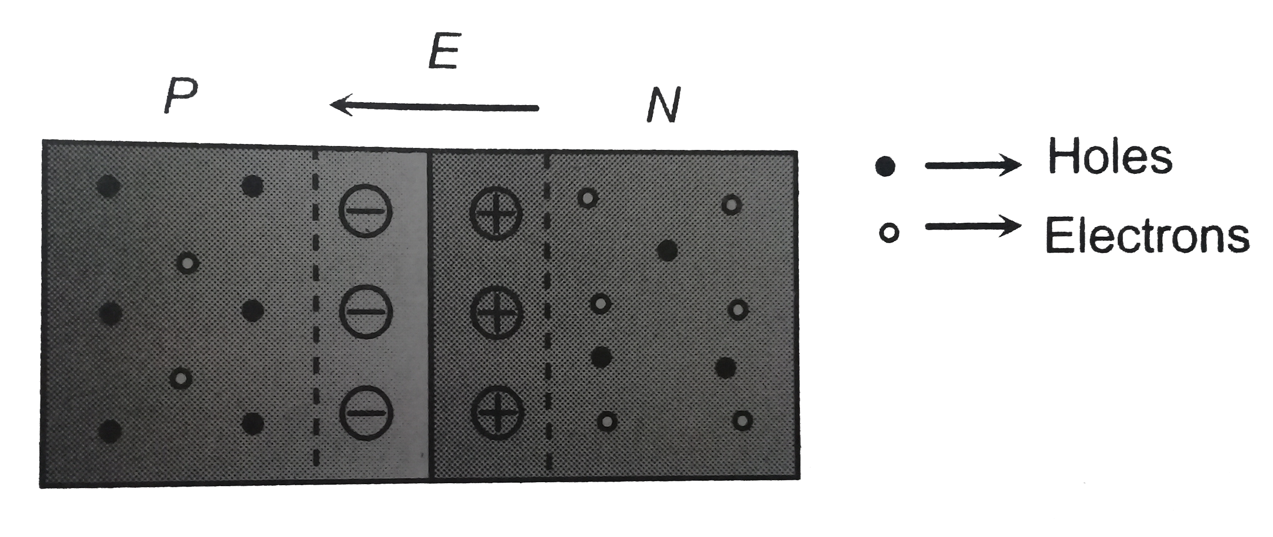
- In a p- n junction diode not connected to any circuit,
Text Solution
|
- Which of the following statements is not true?
Text Solution
|
- The dominant mechanisms for motion of charge carriers in forward and r...
Text Solution
|
- For a given plate voltage , the plate current in a triode valve is max...
Text Solution
|
- The probbility of electrons to be found in the conduction band of an i...
Text Solution
|
- The typical ionisation energy of a donor in silicon is
Text Solution
|
- In the circuit given below, V(t) is the sinusoidal voltage source, vol...
Text Solution
|
- The circuit shown in following figure contanis two diode D(1) and D(2)...
Text Solution
|
- The following configuration of gate is equivalent to
Text Solution
|
- The output of a NAND gate is 0
Text Solution
|
- We are accustomed to decinnial form of stating numbers. For example 12...
Text Solution
|
- Given below are four logic tage symboles. Those for OR, NOR and NAND a...
Text Solution
|
- Consider a two -input AND gate of figure. Out of the four entries for ...
Text Solution
|
- Given below are symbols for some gates. The OR gate and the AND gate, ...
Text Solution
|
- The junction diode in the following circuit requires a minimum current...
Text Solution
|
- In a silicon transistor, the base current is changed by 20 muA. This r...
Text Solution
|
- Assertion: We can measure the potential barrier of a PN junction by pu...
Text Solution
|
- Assertion: Semiconductor do not obey Ohm's law. Reason: Current is d...
Text Solution
|