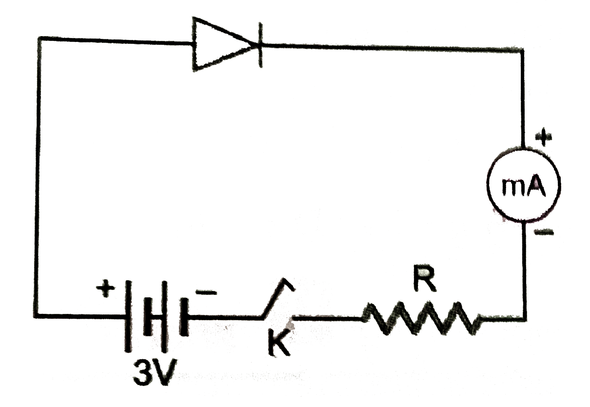
Home
Class 12
PHYSICS
When a p-type semiconductor is brought i...

When a p-type semiconductor is brought into a close contact with n-type semiconductor, we get a p-n junction with a barrier potential `0.4V` and the width of depletion region is `4.0 xx 10^(-7)m`. this p-n junction is forwaed biased with a battery of voltage `3V` adn negligible internal resistance, in series with a resistance of resistance R, ideal milliammeter with reading 20 mA and key K as shown in Fig.

The resistance of resistor R is

A

`1.39xx10^(5) ms^(-1)`

B

`2.78xx10^(5) ms^(-1)`

C

`1.39xx10^(6) ms^(-1)`

D

`2.78xx10^(6) ms^(-1)`

Text Solution

Verified by Experts

The correct Answer is:
A

Let `v_(1)` be the speed of electron when enters the depletion region and `v_(2)` is the speed when it comes out of depletion layer. According to principle of conservation of total energy,
K.E. of the incident electron =workdone against potential barrier +K.E. of the emerging electron.
i.e. `1/2mv_(1)^(2)=eV_+1/2mv_(2)^(2)`
or `1/2xx(9.1xx10^(-31))xx(4xx10^(5))^(2)`
`=(1.6xx10^(-19)xx(0.4)+1/2xx9.1xx10^(-31)xxv_(2)^(2)`
on solving, we get, `v_(2)=1.39xx10^(5) ms^(-1)`
Promotional Banner

Topper's Solved these Questions

  • ELECTRONIC DEVICES

    PRADEEP|Exercise INTEGER TYPE QUESTION|2 Videos
  • ELECTRONIC DEVICES

    PRADEEP|Exercise MULTIPLE CHOICE QUESTIONS|2 Videos
  • ELECTRONIC DEVICES

    PRADEEP|Exercise PROBLEMS FOR PRACTICE|7 Videos
  • ELECTROMAGNETIC WAVES

    PRADEEP|Exercise II Focus multiple choice question|5 Videos
  • ELECTROSTATICS

    PRADEEP|Exercise ASSERTION-REASON TYPE QUESTIONS|2 Videos

Similar Questions

Explore conceptually related problems

When a p-type semiconductor is brought into a close contact with n-type semiconductor, we get a p-n junction with a barrier potential 0.4V and the width of depletion region is 4.0 xx 10^(-7)m . this p-n junction is forwaed biased with a battery of voltage 3V adn negligible internal resistance, in series with a resistance of resistance R, ideal milliammeter and key K as shown in Fig. The resistance of resistor R is

When a p-type semiconductor is brought into a close contact with n-type semiconductor, we get a p-n junction with a barrier potential 0.4V and the width of depletion region is 4.0 xx 10^(-7)m . this p-n junction is forwaed biased with a battery of voltage 3V adn negligible internal resistance, in series with a resistance of resistance R, ideal milliammeter and key K as shown in Fig. The intensity of the electric field in the depletion region when p-n junction is unbiased is

When n and p-type semiconductors are allowed to come into contact

In a p-n junction , the barrier potential offers resistance to

In P-N junction, the barrier potential offerse resistance to

Can we take one slab of p - type semiconductor and physically join it to another n - type semiconductor to get p - n junction?

Semiconductor || P-N junction

Types and Uses OF Semiconductor P-N Junction

The increase in the width of the depletion region in a p-n junction diode is due to: