A
B
C
D
Text Solution
Verified by Experts
The correct Answer is:


Topper's Solved these Questions
Similar Questions
Explore conceptually related problems
MARVEL PUBLICATION-SEMICONDUCTORS -MCQs
- In the case of a p-n junction diode, if the reverse bias is very high,...
Text Solution
|
- What happens to the depletion region of a p-n junction ?
Text Solution
|
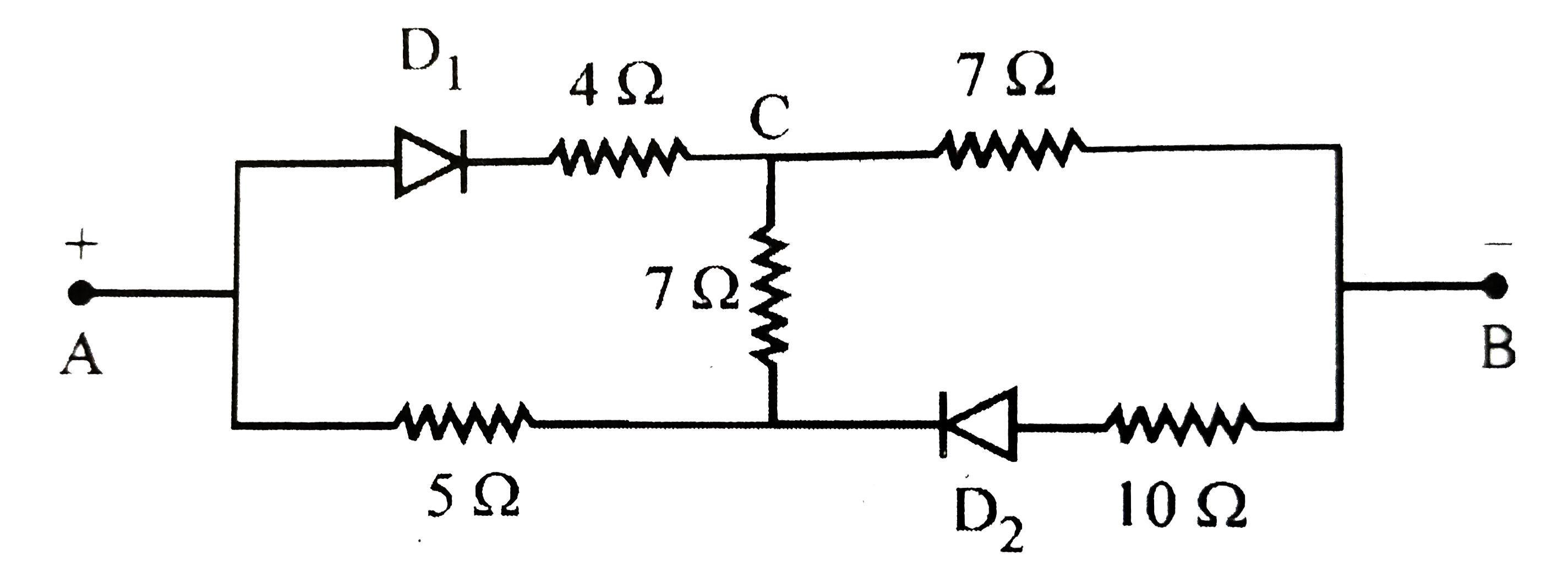
- What is the resistance of the diode circuit between A and B. (D1 and D...
Text Solution
|
- In a p-n junction, the thickness of the depletion region is 10^(-5) m....
Text Solution
|
- A potential barrier of 0.3 V exists across a p-n junction. If the depl...
Text Solution
|
- The potential barrier of a semiconductor is 0.6 Vat room temperature. ...
Text Solution
|
- The current through the diode in the given circuit is
Text Solution
|
- When the P end of P-N junction is connected to the negative terminal o...
Text Solution
|
- The electrical circuit used to get smooth dc output from a rectifier c...
Text Solution
|
- What is the current through an ideal p-n junction diode shown in figur...
Text Solution
|
- What is the current in the following diode circuit?
Text Solution
|
- The depletion layer in P-N junction region is caused by
Text Solution
|
- A junction diode has a resistance of 25 Omega when forward biased and...
Text Solution
|
- When forward bias is applied to a P-N junction, then what happence to ...
Text Solution
|
- In an unbiased p-n junction,
Text Solution
|
- The diode shown in the circuit is a silicon diode. The potential diffe...
Text Solution
|
- A diode having potential difference 0.5 V across its junction which do...
Text Solution
|
- In a reverse biased diode, when the applied voltage changes by 1V, the...
Text Solution
|
- Barrier potential of a p-n junction diode does not depend on
Text Solution
|
- When p-n junction diode is forward biased then
Text Solution
|