Home
Class 12
PHYSICS
For a NAND gate the inputs and outputs f...

For a NAND gate the inputs and outputs for different time invervals are given below :

The values taken by P,Q,R,S are respectively

A

1,0,1,1

B

1,1,1,0

C

0,1,0,1

D

0,1,0,0

Text Solution

Verified by Experts

The correct Answer is:
B

The truth table of the NAND gate is given as

`therefore` The values of P,Q,R,S are (1,1,1,0)
Promotional Banner

Topper's Solved these Questions

  • ROTATIONAL MOTION

    MARVEL PUBLICATION|Exercise TEST YOUR GRASP - 3|8 Videos
  • STATIONARY WAVES

    MARVEL PUBLICATION|Exercise TEST YOUR GRASP-8|20 Videos

Similar Questions

Explore conceptually related problems

The inputs and outputs for different time intervals are given below for NAND gate The value taken by P, Q, R, S are respectively

Sketch inputs A,B and output Y from a NAND gate from the table given below

The symbolic representation of four logic gates are given below : The logic symbols for OR, NOT and NAND gates are respectively :

The symbolic representation of four logic gates are given below : The logic symbols for OR, NOT and NAND gates are respectively :-

If pto(q ^^ r) is false, then the truth values of p,q and r are respectively

A NOR gate and a NAND gate are connected shown. Two different sets of inputs are given to this set up. In the first case, the inputs to the gates are A = 0, B = 0, C = 0. In the second case, the inputs are A = 1, B = 0, C = 1. The output D in the first case and second case respectively are

Let a:~(p ^^ ~r) vv (~ q vv s ) and b:(p vv s ) lar (q ^^ r) . If the truth values of p and q are true and that of r and s are false, then the truth values of a and b are respectively . . .

Given below are symbols for some gates. The OR gate and the AND gate, respectively are

If the truth value of the statement p to (~q vee r) is false (F), then the truth values of the statements p,q and r are respectively

To get output ‘0’ at R, for the given logic gate circuit the input values must be:

MARVEL PUBLICATION-SEMICONDUCTORS -MCQs
  1. If the Output of two NAND gates is given to input of a NAND gate. Then...

    Text Solution

    |

  2. In the circuit below, A and B represents two inputs and C represents t...

    Text Solution

    |

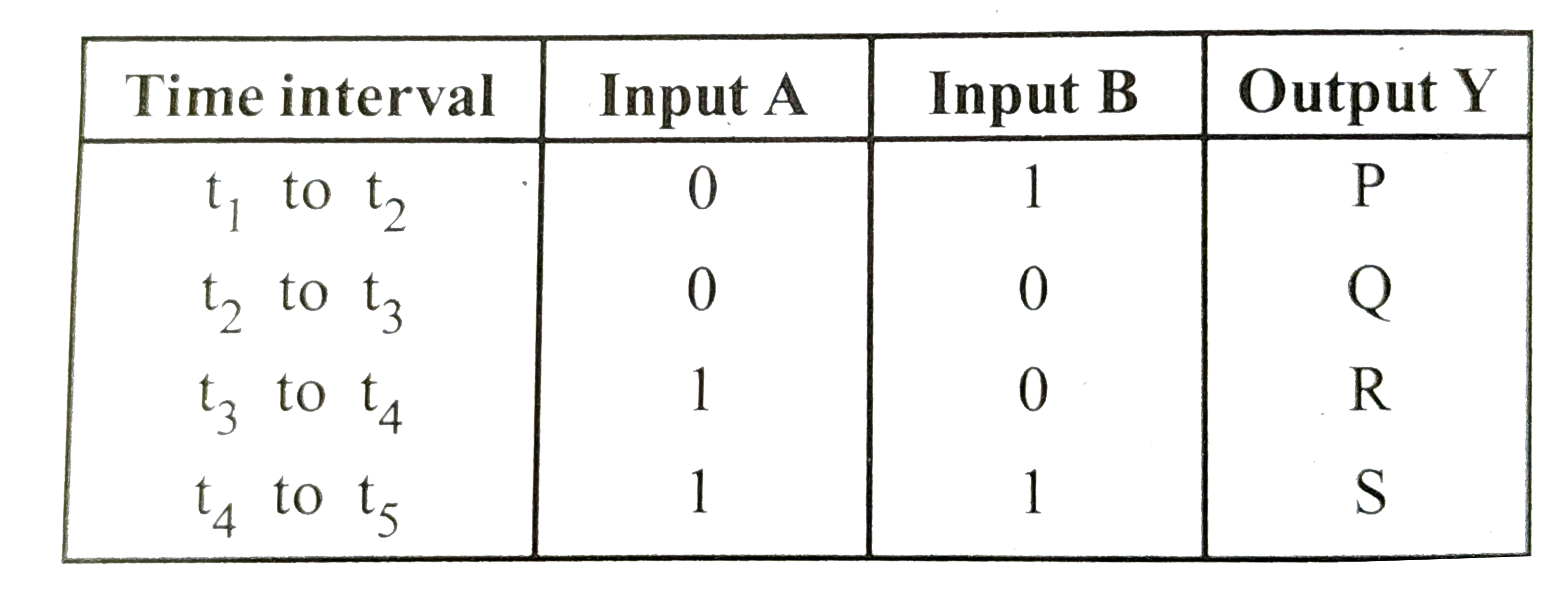
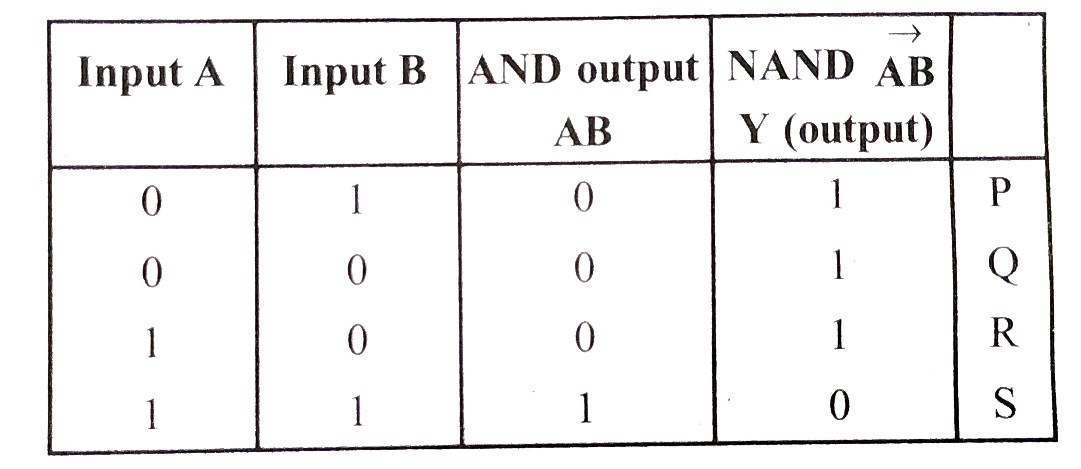
  3. For a NAND gate the inputs and outputs for different time invervals ar...

    Text Solution

    |

  4. The output y, when all three inputs are first high and then low, will ...

    Text Solution

    |

  5. In the following circuit, the output Y for all possible inputs A and B...

    Text Solution

    |

  6. The combination of the 'NAND' gates shown here (Fig.) and (ii)) are eq...

    Text Solution

    |

  7. The temperature (T) dependence of resistivity (rho) of a semiconductor...

    Text Solution

    |

  8. A full wave rectifier circuit along with the input and output are show...

    Text Solution

    |

  9. A p-n junction (D) shown in the figure can act as a rectifier. An alte...

    Text Solution

    |

  10. If a p-n junction diode, a square input signal of 10 V is applied as s...

    Text Solution

    |

  11. A hole in a P - type semiconductor is

    Text Solution

    |

  12. Colour of light emitted by LED depends upon

    Text Solution

    |

  13. In a semiconductor , acceptor imparity is

    Text Solution

    |

  14. In an oscillator, for sustained oscillations, Barkhausen criterion is ...

    Text Solution

    |

  15. The depletion region of p-n junction has a thickness of the order of

    Text Solution

    |

  16. Which logic gate corresponds to the truth table given below ?

    Text Solution

    |

  17. A light emitting diode is shown as

    Text Solution

    |

  18. For a transistor , alpha(dc) and beta(dc) are the current ratios, t...

    Text Solution

    |

  19. Photodiode is a device

    Text Solution

    |

  20. The energy band gap is maximum in

    Text Solution

    |