


MARVEL PUBLICATION-SEMICONDUCTORS -MCQs
- The depletion region of p-n junction has a thickness of the order of
Text Solution
|
- Which logic gate corresponds to the truth table given below ?
Text Solution
|
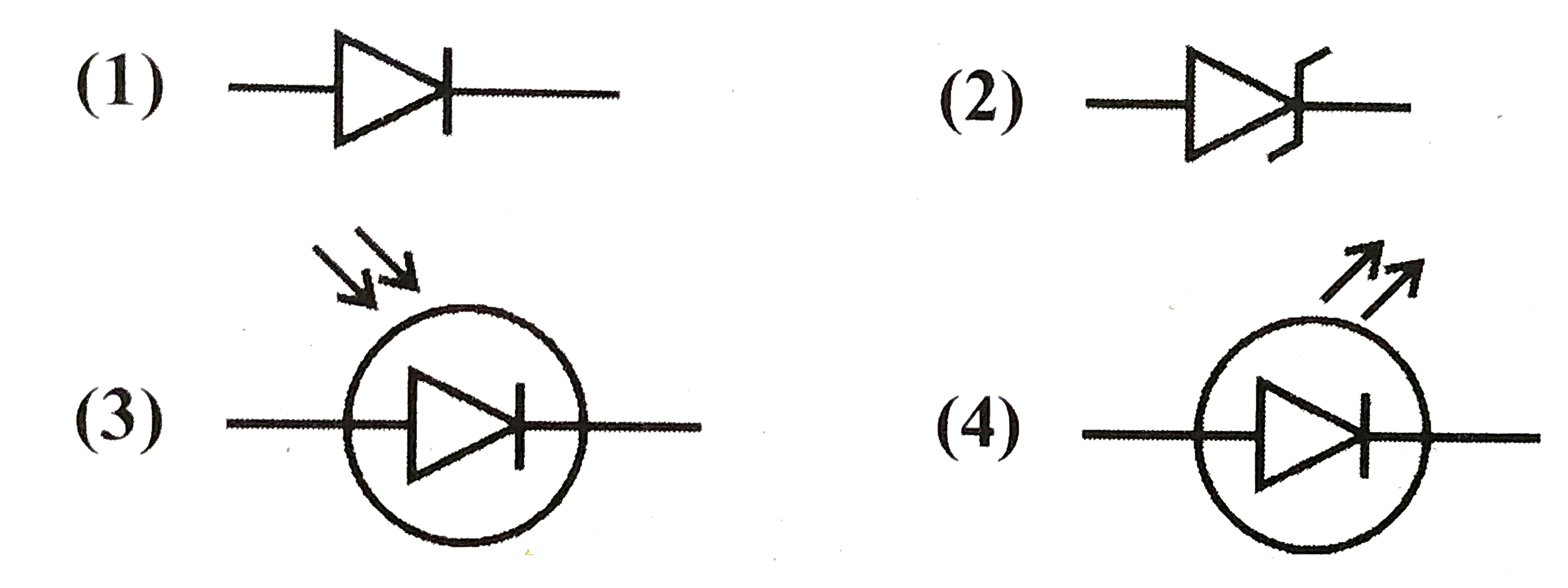
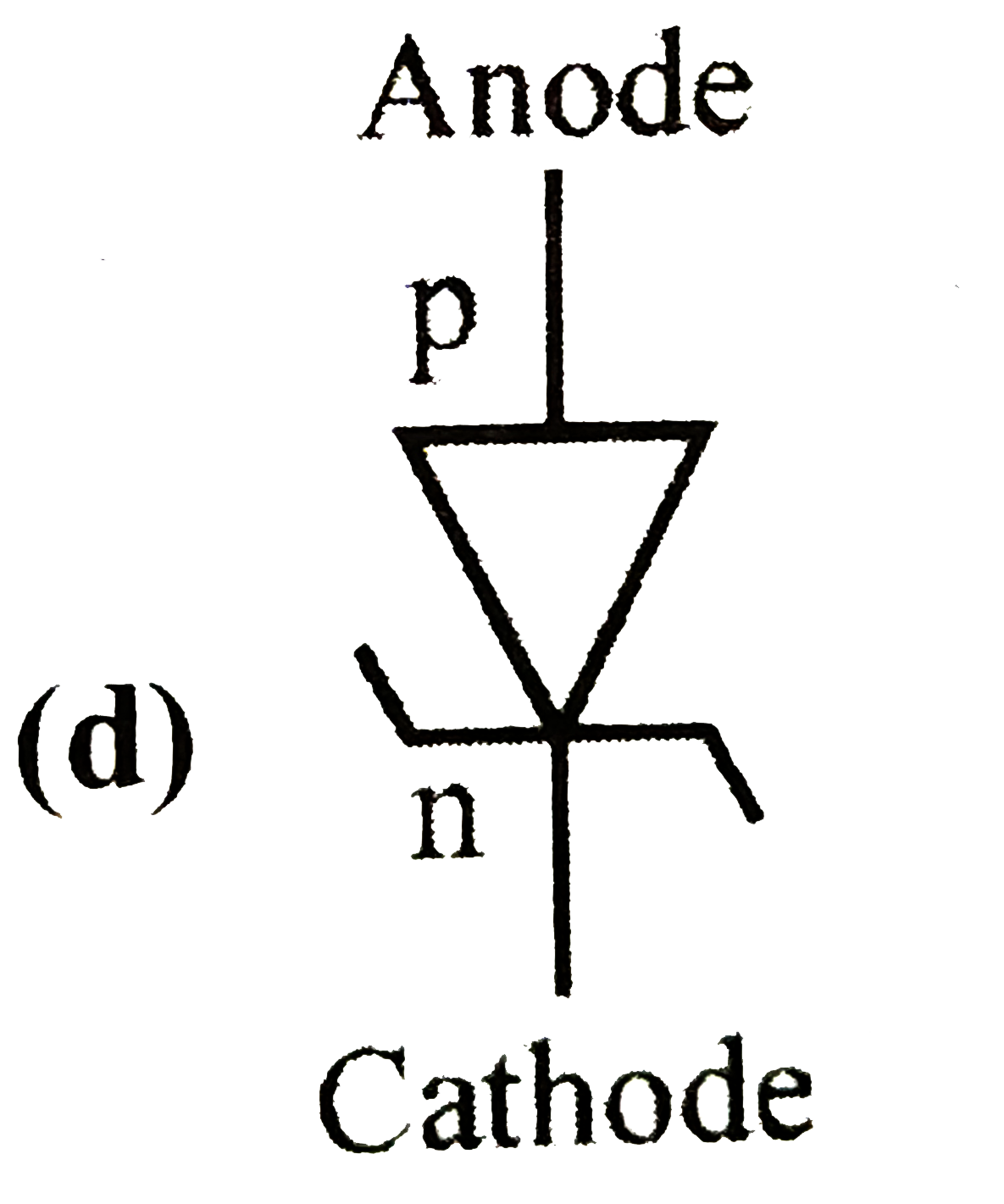
- A light emitting diode is shown as
Text Solution
|
- For a transistor , alpha(dc) and beta(dc) are the current ratios, t...
Text Solution
|
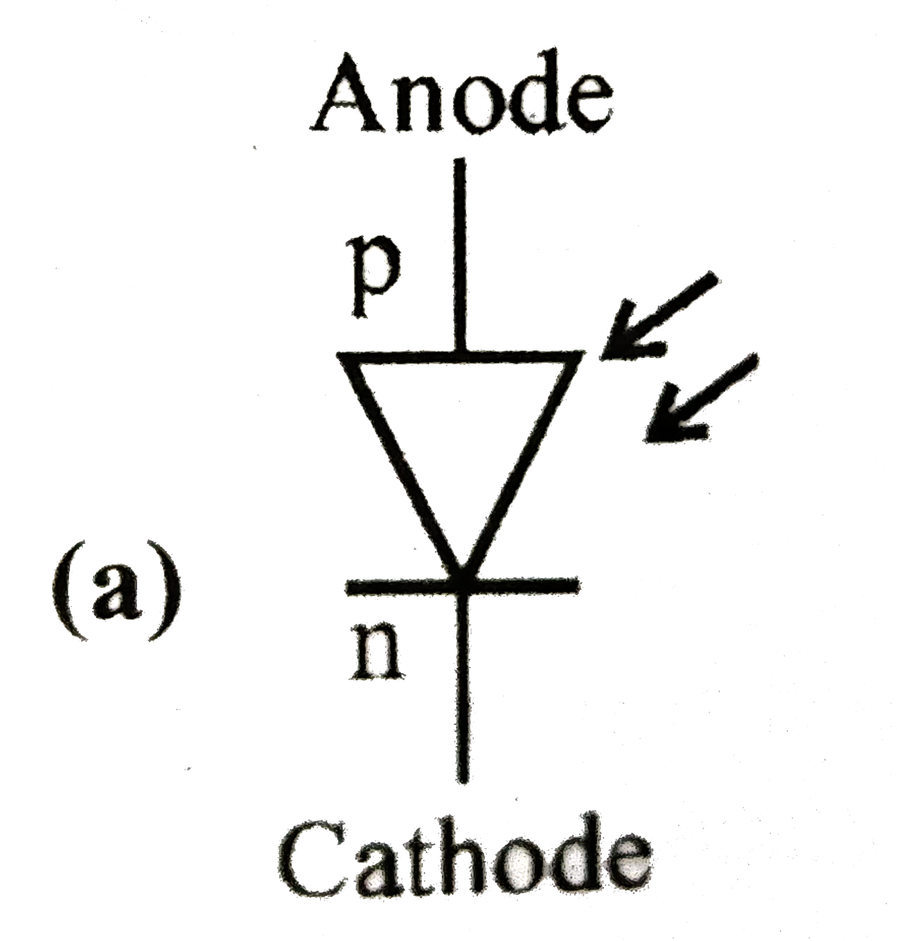
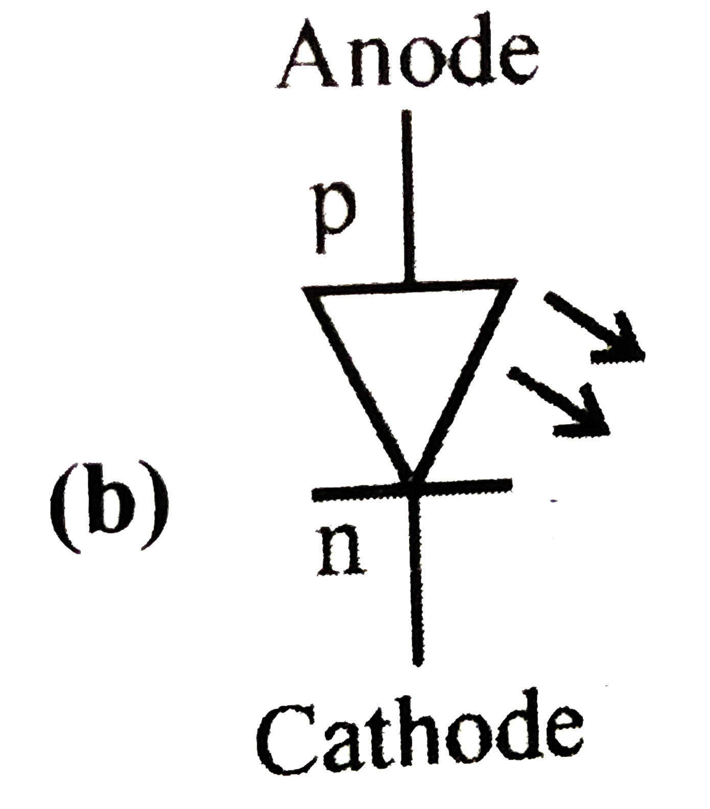
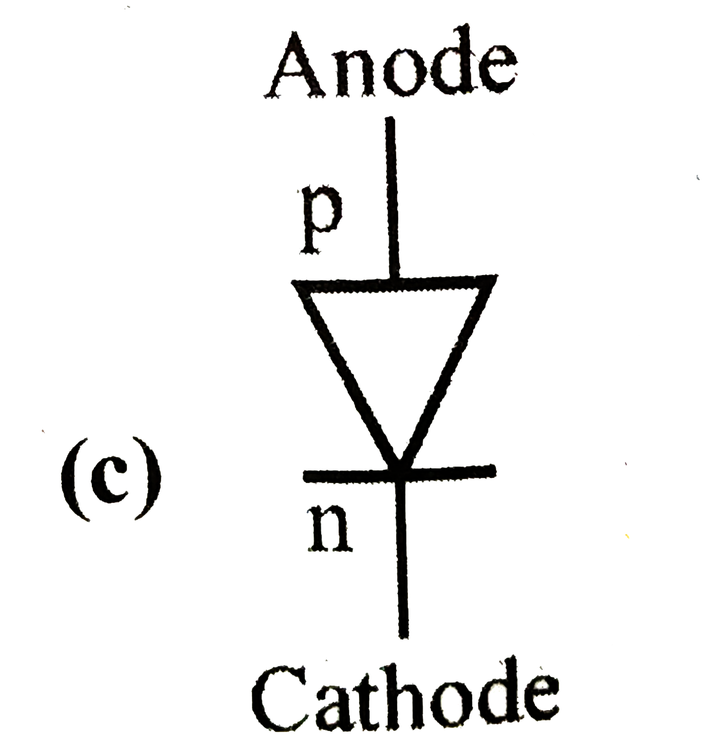
- Photodiode is a device
Text Solution
|
- The energy band gap is maximum in
Text Solution
|
- INTRINSIC SEMICONDUCTORS
Text Solution
|
- A semiconductor is known to have an electron concentration of 5 xx 10^...
Text Solution
|
- When arsenic is added as an impurity to silicon, the resulting materia...
Text Solution
|
- which one of the following statements is wrong ?
Text Solution
|
- In a p-n junction, the thickness of the depletion layer is 10^(-6) m. ...
Text Solution
|
- What is the current in the following junction diode circuit?
Text Solution
|
- A p-n junction diode has a forward bias resistance of 10Omega and a re...
Text Solution
|
- The width of the depletion region in a p-n junction diode is 400 nm an...
Text Solution
|
- The circuit has two oppositely connected ideal diodes in parallel. Wha...
Text Solution
|
- State the reason, why GaAs is most commonly used in making of a solar ...
Text Solution
|
- Avalanche breakdown is due to
Text Solution
|
- A P-N photodiode is fabricated from a semiconductor with a band gap of...
Text Solution
|
- What is the current flowing through 1 KOmega restsor in the following...
Text Solution
|
- For a transistor, beta = 50. Input resistance (Ri) = 200Omega. Output ...
Text Solution
|