 .
.Text Solution
Verified by Experts


Topper's Solved these Questions
SEMI CONDUCTOR DEVICES
NARAYNA|Exercise C.U.Q|155 VideosSEMI CONDUCTOR DEVICES
NARAYNA|Exercise Level-I (C.W)|21 VideosRAY OPTICS AND OPTICAL INSTRAUMENTS
NARAYNA|Exercise EXERCISE- 4 One or more than one correct answer type|13 VideosSEMICONDUCTOR ELECTRONICS
NARAYNA|Exercise ADDITIONAL EXERCISE (ASSERTION AND REASON TYPE QUESTIONS :)|19 Videos
Similar Questions
Explore conceptually related problems
NARAYNA-SEMI CONDUCTOR DEVICES-Level-II (H.W)
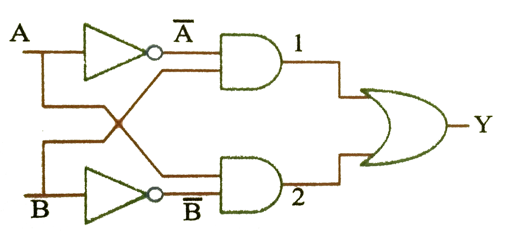
- The Boolean expression of the output Y of the inputs A and B for the c...
Text Solution
|
- If the lattice constant of this semiconductor is decreased, then which...
Text Solution
|
- A Ge specimen is dopped with Al. The concentration of acceptor atoms i...
Text Solution
|
- The following data are for intrinsic germanium at 300 K. n(i) = 2.4 xx...
Text Solution
|
- The diagram correctly represents the direction of flow of charge carri...
Text Solution
|
- In the figure shown below .
Text Solution
|
- A P-N junction diode can withstand currents up to 10 mA. Under forward...
Text Solution
|
- A cell of emf. 4.5 V is connected to a junction diode whose barrier po...
Text Solution
|
- V(A) and V(B) denote potential of A and B, then the equivalent resista...
Text Solution
|
- Two ideal junction diodes D(1),D(2) are connected as shown in the figu...
Text Solution
|
- Find the effective resistance between A and B .
Text Solution
|
- The peak voltage in the output of a half-wave diode rectifier fed with...
Text Solution
|
- In the figure shown the potential drop across the series resistor is
Text Solution
|
- A 220 V AC supply is connected between points A and B . What will be t...
Text Solution
|
- In the circuit shown(Fig.) if the diode forward voltage drop is 0.3 V,...
Text Solution
|
- In an n-p-n transistor 10^(10) electrons enter the emitter in 10^(-6)s...
Text Solution
|
- In a common base mode of transistor, collector current is 5.488 mA for...
Text Solution
|
- Current amplification factor of a common base configuration is 0.88. F...
Text Solution
|
- For a transistor beta = 40 and I(B) = 25 muA. Find the value of I(E).
Text Solution
|
- In a transistor if (I(C))/(I(E))=alpha and (I(C))/(I(B))=beta,If alpha...
Text Solution
|
- For a transistor x=(1)/(alpha)&y=(1)/(beta) where alpha & beta are cur...
Text Solution
|