A

B

C

D

Text Solution
Verified by Experts
The correct Answer is:


Topper's Solved these Questions
SEMI CONDUCTOR DEVICES
NARAYNA|Exercise Level-III (C.W)|20 VideosSEMI CONDUCTOR DEVICES
NARAYNA|Exercise NCERT (Comprehension)|13 VideosSEMI CONDUCTOR DEVICES
NARAYNA|Exercise Level-I (C.W)|21 VideosRAY OPTICS AND OPTICAL INSTRAUMENTS
NARAYNA|Exercise EXERCISE- 4 One or more than one correct answer type|13 VideosSEMICONDUCTOR ELECTRONICS
NARAYNA|Exercise ADDITIONAL EXERCISE (ASSERTION AND REASON TYPE QUESTIONS :)|19 Videos
Similar Questions
Explore conceptually related problems
NARAYNA-SEMI CONDUCTOR DEVICES-Level-II (C.W)
- A p-n junction (D) shown in the figure can act as a rectifier. An alte...
Text Solution
|
- In the diagram, the input is across the terminals A and C and the outp...
Text Solution
|
- The I-V characteristic of an LED is.
Text Solution
|
- In the circuit shown. The potential drop across each capacitor is (ass...
Text Solution
|
- The maximum and minimum values of zener diode current are
Text Solution
|
- In an n-p-n transistor circuit, the collector current ia 10 mA. If 90%...
Text Solution
|
- The constant alpha of a transistor is 0.9 What would be the change in ...
Text Solution
|
- A voltage amplifier operated from a 12 volt battery has a collector lo...
Text Solution
|
- In a transistor circuit shown here the base current is 35 muA. The val...
Text Solution
|
- In a single state transistor amplifier, when the signal changes by 0.0...
Text Solution
|
- On subtracting 010101 from 101010, we get :
Text Solution
|
- The minimum number of gates required to realise this expression Z = DA...
Text Solution
|
- In the circuit below, A and B represents two inputs and C represents t...
Text Solution
|
- In the following circuit the output Y becomes zero for the inputs .
Text Solution
|
- The combination of gates shown below yields .
Text Solution
|
- The logic gate having an output of 1 is. (i)
Text Solution
|
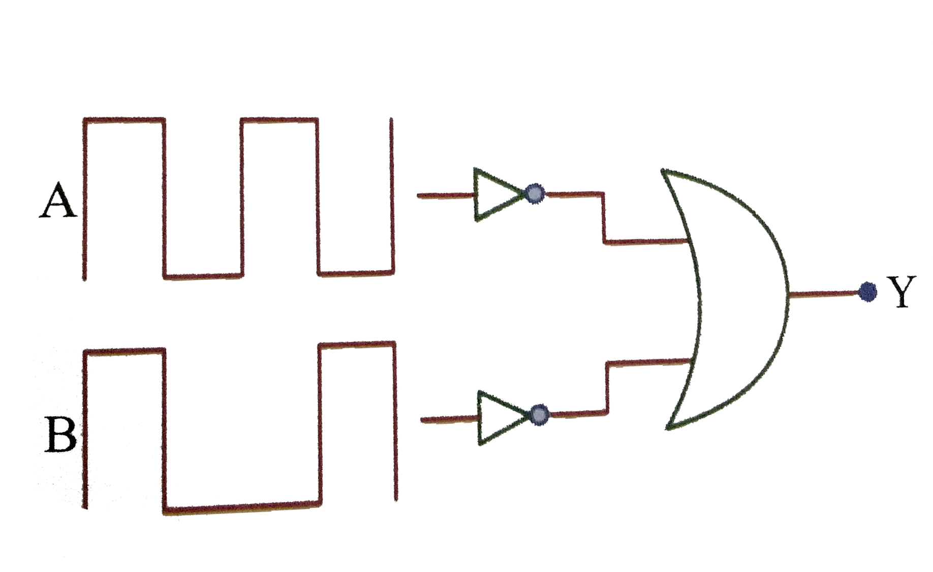
- In a given circuit as shown the two input wave forms A and B are appli...
Text Solution
|
- The output of the combination of the gates shown in the figure below i...
Text Solution
|
- The expression of Y in following circuit is .
Text Solution
|
- How many NAND gate are used to from AND gate?
Text Solution
|