A
B
C
D
Text Solution
Verified by Experts
The correct Answer is:


Topper's Solved these Questions
ELECTRONICS
ERRORLESS |Exercise Digital Electronics|2 VideosELECTRONICS
ERRORLESS |Exercise Valve Electronics (Diode and Triode)|3 VideosELECTRON, PHOTON, PHOTOELECTRIC EFFECT AND X-RAYS
ERRORLESS |Exercise Self Evaluation Test|3 VideosELECTROSTATICS
ERRORLESS |Exercise Ordinary Thinking Objective Questions (Electric Flux and Gauss.s Law)|28 Videos
Similar Questions
Explore conceptually related problems
ERRORLESS -ELECTRONICS-Selv Evaluation Test
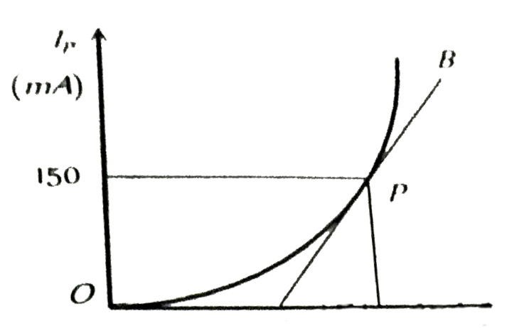
- The plate characteristic curve of a diode in space charge limited regi...
Text Solution
|
- In a pure silicon (n(i)=10^(16)//m^(3)) crystal at 300K, 10^(21) atoms...
Text Solution
|
- In the Boolean algebra bar(A).bar(B) equals is :-
Text Solution
|
- In the given circuit as shown the two input waveform A and B are appli...
Text Solution
|
- Two identical capacitors A and B are charged to the same potential V a...
Text Solution
|
- In transistor, forward bias is always smaller than the reverse bias. T...
Text Solution
|
- In NPN transistor, if doping in base region is increased then collecto...
Text Solution
|
- In the following circuit I(1) and I(2) are respectively
Text Solution
|
- In space charge limited region, the plate current in a diode is 10 mA ...
Text Solution
|
- A triode has a plate resistance of 10 k Omega and amplification factor...
Text Solution
|
- Pure sodium (Na) is a good conductor of electricity because the 3s and...
Text Solution
|
- Would there be any advantage to adding n-type or p-type impurities to ...
Text Solution
|
- In the following common emitter circuit if beta=100, V(CE)=7 V, V(BE)=...
Text Solution
|
- When a battery is connected to a P-type semiconductor with a metallic ...
Text Solution
|
- Is the ionisation energy of an isolated free atom different from the i...
Text Solution
|
- In the following circuit, a voltmeter V is connected across a lamp L. ...
Text Solution
|
- For given electric voltage signal dc value is
Text Solution
|
- When a silicon PN junction is in forwards biased condition with series...
Text Solution
|
- In the following circuit the equivalent resistance between A and B is
Text Solution
|
- In the following circuit of PN junction diodes D(1),D(2) and D(3) are ...
Text Solution
|
- In circuit in following figure the value of Y is-
Text Solution
|