Home
Class 12
PHYSICS
The output of the given circuit in figur...

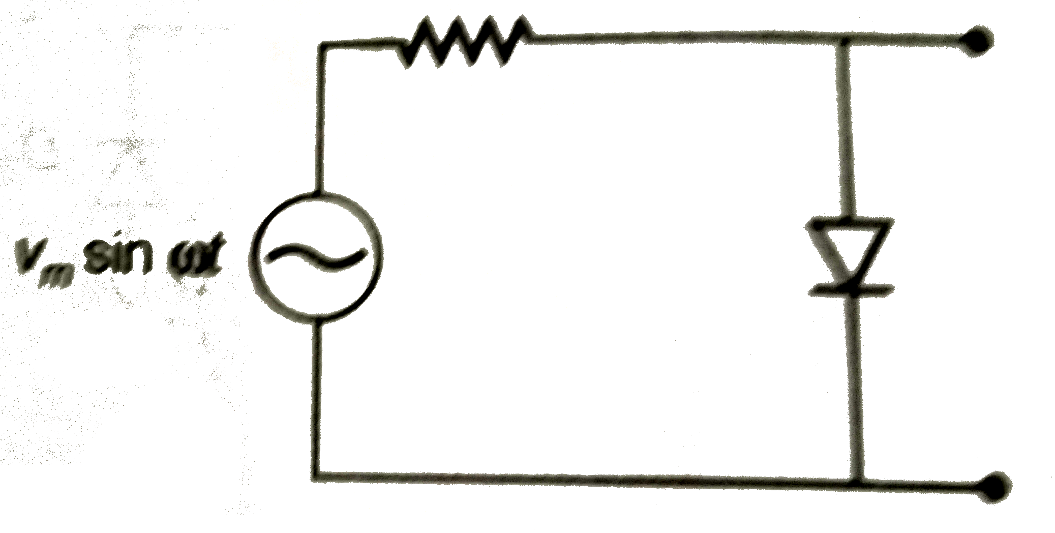
The output of the given circuit in figure given below,

A

would be zero at all times

B

would be like a half wave rectifier with positive cycles in output

C

would be like a half wave rectifier with negative cycles in ouput

D

would be like that of a full wave reactifier.

Text Solution

Verified by Experts

The correct Answer is:
C

Due to forward biased during positive half cycle of input AC voltage, the resistance of `p - n` junction is low. The current in the circuit is maximum. In this situation, a maximum potential difference will appear across resistance connected in series of circuit. This result into zero output voltage across `p - n` junction.
Due to reverse bisase during negative half cycle of AC voltage, the `p - n` junction is reverse biased. The resistance of `p - n` junction becomes high which will be more than resistance in series. That is why, there will be voltage across `p - n` junction with negative cycle in output.
Promotional Banner

Topper's Solved these Questions

  • MOVING CHARNGES AND MAGNETISM

    NCERT EXEMPLAR|Exercise Moving Charnges And Magnetism|29 Videos
  • RAY OPTICS AND OPTICAL INSTRUMENTS

    NCERT EXEMPLAR|Exercise Ray Optics And Optical Instruments|32 Videos

Similar Questions

Explore conceptually related problems

The output of the given circuit,is

The output for the given, circuit is

In the given circuit figure

The output of the given logic circuit is

The output of given logic circuit is

The output of the given logic circuit is :

The output of given logic circuit is

The output Y of the gate circuit shown in the figure below is

The output Y of the gate circuit shown in the figure below is

The output Y of the logic circuit given below is

NCERT EXEMPLAR-NUCLEI-Nuclei
  1. A 220 V AC supply is connected between points A and B . What will be t...

    Text Solution

    |

  2. Hole is

    Text Solution

    |

  3. The output of the given circuit in figure given below,

    Text Solution

    |

  4. In the circuit shown in figure, if the diode forward voltage drop is 0...

    Text Solution

    |

  5. Truth table for the given circuit (Fig.)is

    Text Solution

    |

  6. When an electric field is applied across a semiconductor,

    Text Solution

    |

  7. Consider an n-p-n transistor with its base - emitter junction forward ...

    Text Solution

    |

  8. Fig.shows that transfer characteristics of a base biased CE transistor...

    Text Solution

    |

  9. In a n - p - n transistor circuit, the collector current is 10 mA. If ...

    Text Solution

    |

  10. In the depletion region of a diode.

    Text Solution

    |

  11. What happens during regualtion action of a Zener diode?

    Text Solution

    |

  12. To reduce the ripples in rectifier circuit with capacitor filter

    Text Solution

    |

  13. The breakdown in a reverse biased p-n junction diode is more likely to...

    Text Solution

    |

  14. Why are elemental dopants for Silicon or Germanium usually chosen fro...

    Text Solution

    |

  15. Sn, C, Si and Ge are all group XIV elements . Yet , Sn is a conductor ...

    Text Solution

    |

  16. Can the potential barrier across a p - n junction be measured by simpl...

    Text Solution

    |

  17. Draw the output waveform across the resistor (Fig.)

    Text Solution

    |

  18. The amplifiers X, Y and Z are connected in series. If the voltage gain...

    Text Solution

    |

  19. In a CE transistor amplifier, there is a current and voltage gain asso...

    Text Solution

    |

  20. (i) Name the type of a diode whose characteristics are shown in figure...

    Text Solution

    |