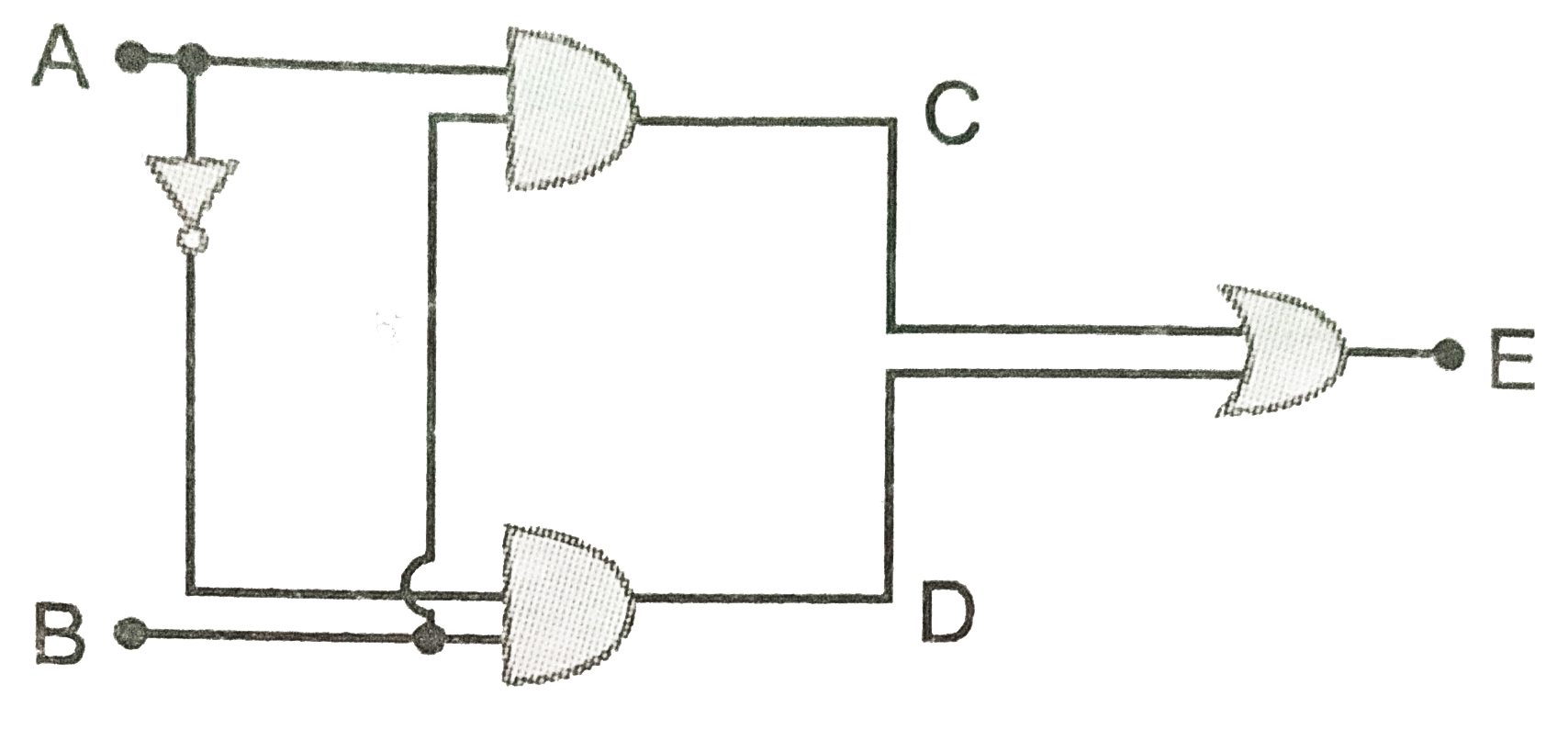
A
B
C
D
Text Solution
Verified by Experts
The correct Answer is:


Topper's Solved these Questions
Similar Questions
Explore conceptually related problems
NCERT EXEMPLAR-NUCLEI-Nuclei
- The output of the given circuit in figure given below,
Text Solution
|
- In the circuit shown in figure, if the diode forward voltage drop is 0...
Text Solution
|
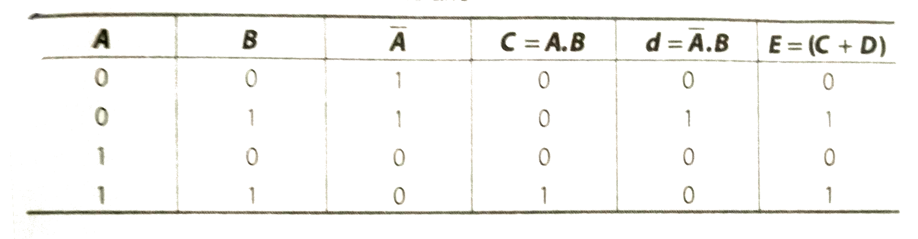
- Truth table for the given circuit (Fig.)is
Text Solution
|
- When an electric field is applied across a semiconductor,
Text Solution
|
- Consider an n-p-n transistor with its base - emitter junction forward ...
Text Solution
|
- Fig.shows that transfer characteristics of a base biased CE transistor...
Text Solution
|
- In a n - p - n transistor circuit, the collector current is 10 mA. If ...
Text Solution
|
- In the depletion region of a diode.
Text Solution
|
- What happens during regualtion action of a Zener diode?
Text Solution
|
- To reduce the ripples in rectifier circuit with capacitor filter
Text Solution
|
- The breakdown in a reverse biased p-n junction diode is more likely to...
Text Solution
|
- Why are elemental dopants for Silicon or Germanium usually chosen fro...
Text Solution
|
- Sn, C, Si and Ge are all group XIV elements . Yet , Sn is a conductor ...
Text Solution
|
- Can the potential barrier across a p - n junction be measured by simpl...
Text Solution
|
- Draw the output waveform across the resistor (Fig.)
Text Solution
|
- The amplifiers X, Y and Z are connected in series. If the voltage gain...
Text Solution
|
- In a CE transistor amplifier, there is a current and voltage gain asso...
Text Solution
|
- (i) Name the type of a diode whose characteristics are shown in figure...
Text Solution
|
- Three photodiodes D1 , D2 and D3 are made of semiconductors having ...
Text Solution
|
- If the resistance R(1) is increased (see figure), how will the reading...
Text Solution
|