Text Solution
Verified by Experts


Topper's Solved these Questions
SEMICONDUCTOR ELECTRONICS METERIALS DEVICES AND SIMPLE CIRCUITS
MODERN PUBLICATION|Exercise REVISION EXERCISES (VERY SHORT ANSWER QUESTION)|61 VideosSEMICONDUCTOR ELECTRONICS METERIALS DEVICES AND SIMPLE CIRCUITS
MODERN PUBLICATION|Exercise REVISION EXERCISES (ADDITOINAL QUESTION)|9 VideosSEMICONDUCTOR ELECTRONICS METERIALS DEVICES AND SIMPLE CIRCUITS
MODERN PUBLICATION|Exercise NCERT FILE SOLVED (TEXT BOOK EXERCISES )|30 VideosRAY OPTICS AND OPTICAL INSTRUMENTS
MODERN PUBLICATION|Exercise CHAPTER PRACTICE TEST|14 VideosWAVE OPTICAL
MODERN PUBLICATION|Exercise CHAPTER PRACTICE TEST|7 Videos
Similar Questions
Explore conceptually related problems
MODERN PUBLICATION-SEMICONDUCTOR ELECTRONICS METERIALS DEVICES AND SIMPLE CIRCUITS -HIGER ORDER THINKING SKILLS & ADVANCED LEVEL
- Impurity levels in a doped semiconductor is found to be 35 millielectr...
Text Solution
|
- In semiconductors, thermal collisions are responsible for taking a val...
Text Solution
|
- When a p-type impurity is doped in a semiconductor,a large number of h...
Text Solution
|
- A zener diode of power rating 2 W is to used as a voltage regulator if...
Text Solution
|
- If the two ends of a p-n junction are joined by a wire will there be s...
Text Solution
|
- Calculate the number of states per cubic metre of sodium in 3s band. T...
Text Solution
|
- A semiconductor material x is made by doping a germanium crystal with...
Text Solution
|
- A student constructed an inexpensive lamp using a diode to allow light...
Text Solution
|
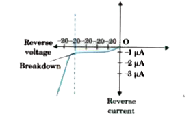
- A photodiode is operated in reverse mode under different illuminatio...
Text Solution
|
- The lattice structure for both carbon and silicon is same with each o...
Text Solution
|
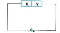
- The ideal diodes D(1) and D(2) are to be connected in the positions sh...
Text Solution
|