Text Solution
Verified by Experts


Topper's Solved these Questions
SEMICONDUCTOR ELECTRONICS : MATERIALS , DEVICES AND SIMPLE CIRCUITS
NEW JOYTHI PUBLICATION|Exercise SOLUTION TO EXERCISES FROM NCERT TEXT|17 VideosSEMICONDUCTOR ELECTRONICS : MATERIALS , DEVICES AND SIMPLE CIRCUITS
NEW JOYTHI PUBLICATION|Exercise PRACTICE PROBLEMS FOR SELF ASSESSMENT|8 VideosRAY OPTICS AND OPTICAL INSTRUMENTS
NEW JOYTHI PUBLICATION|Exercise COMPETITIVE EXAM CORNER|26 VideosWAVE OPTICS
NEW JOYTHI PUBLICATION|Exercise COMPETITIVE EXAM CORNER|17 Videos
Similar Questions
Explore conceptually related problems
NEW JOYTHI PUBLICATION-SEMICONDUCTOR ELECTRONICS : MATERIALS , DEVICES AND SIMPLE CIRCUITS -COMPETITIVE EXAM CORNER
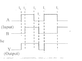
- Justify the output waveform (Y) of the OR gate for the following input...
Text Solution
|
- A pure semiconductor has equal electron and hole concentration of 10^(...
Text Solution
|
- The collector supply voltage is 6 V and the voltage drop across a resi...
Text Solution
|
- A full - wave rectifier circuit with an ac input is shown. The ou...
Text Solution
|
- When the voltage drop across a p-n junction diode is increased from 0...
Text Solution
|
- If the voltage between the terminals A and B is 17 V and Zener breakdo...
Text Solution
|
- GaAs (with a band gap = 1.5 eV) as a L.E.D can emit
Text Solution
|
- The circuit diagram shows a logic combination with the states of outpu...
Text Solution
|
- In a common emitter transistor amplifier , the output resistance is 50...
Text Solution
|
- In the circuit given , the current through the zener diode is
Text Solution
|
- A transistor oscillator is (i) an amplifier with positive feedback (ii...
Text Solution
|
- A semiconductor with a band gap of 2.5 eV is used to fabricate a p-n p...
Text Solution
|
- In the circuit given A , B and C are inputs and Y is the output T...
Text Solution
|
- In the given circuits for ideal diode , the current through the batter...
Text Solution
|
- The logic gates giving output '1' for the inputs of '1' and '0' are
Text Solution
|
- Identify the mismatch of the following :
Text Solution
|
- If a PN junction diode of depletion layer width W and barrier height ...
Text Solution
|
- The heavily and lightly doped regions of a bipolar junction transistor...
Text Solution
|
- The device used for detecting optical signal is
Text Solution
|
- The logical operation carried out by the above circuit is
Text Solution
|
- In CE transistor amplifier , if the base current is increased by 20 mu...
Text Solution
|