Text Solution
Verified by Experts


Topper's Solved these Questions
SEMICONDUCTOR ELECTRONICS : MATERIALS , DEVICES AND SIMPLE CIRCUITS
NEW JOYTHI PUBLICATION|Exercise CONTINUOUS EVALUATION (ASSIGNMENT)|7 VideosSEMICONDUCTOR ELECTRONICS : MATERIALS , DEVICES AND SIMPLE CIRCUITS
NEW JOYTHI PUBLICATION|Exercise PREVIOUS YEAR QUESTIONS|3 VideosSEMICONDUCTOR ELECTRONICS : MATERIALS , DEVICES AND SIMPLE CIRCUITS
NEW JOYTHI PUBLICATION|Exercise PRACTICE PROBLEMS FOR SELF ASSESSMENT|8 VideosRAY OPTICS AND OPTICAL INSTRUMENTS
NEW JOYTHI PUBLICATION|Exercise COMPETITIVE EXAM CORNER|26 VideosWAVE OPTICS
NEW JOYTHI PUBLICATION|Exercise COMPETITIVE EXAM CORNER|17 Videos
Similar Questions
Explore conceptually related problems
NEW JOYTHI PUBLICATION-SEMICONDUCTOR ELECTRONICS : MATERIALS , DEVICES AND SIMPLE CIRCUITS -EVALUATION QUESTIONS AND ANSWER
- The energy gap of diamond is 6 eV . a . What does it mean ? b. Wha...
Text Solution
|
- When impurity (atom) is added to an intrinsic semiconductor , then it ...
Text Solution
|
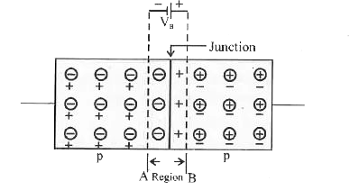
- Fig shows a p-n junction diode. a. What does V(B) denote ? b. N...
Text Solution
|
- What is the value of conductivity of a semiconductor at absolute zero ...
Text Solution
|
- Can a transistor amplifier generate power ?
Text Solution
|
- Give some properties of a semiconductor.
Text Solution
|
- What is a Zener diode ?
Text Solution
|
- What are the characteristics of a hole ?
Text Solution
|
- Copy and complete the following block diagram .
Text Solution
|
- What is meant by forbidden energy gap ?
Text Solution
|
- What do you mean by fermi energy ?
Text Solution
|
- What is depletion region in p-n junction ?
Text Solution
|
- What will happen if both , emitter and collector of a transistor are r...
Text Solution
|
- How does conductivity of a semiconductor increase ?
Text Solution
|
- The forward bias of a diode is wrongly given above . a. Redraw the a...
Text Solution
|
- Classify the following into conductors , insulators and semi conductor...
Text Solution
|
- The magnitude of potential barrier of germanium is about 0.3 V . a W...
Text Solution
|
- a. What type of biasting is used here ? b. What happens to the deple...
Text Solution
|
- Why is a NOT gate known as an inverter ?
Text Solution
|
- a. What type of biasting is used here ? b. What happens to the deple...
Text Solution
|