Home
Class 12
PHYSICS
Explain conductor (metal), insulator and...

Explain conductor (metal), insulator and semiconductor by drawing diagrams based on band.

Text Solution

Verified by Experts

Atomic number of Si is 14. The electron configuration of silicon atom is `1s^(2)2s^(2)2p^(6)3s^(2)3p^(2)` hence K and L shells are completely filled and M shell is incomplete and there are `3s^(2)3p^(2)` valence electron in it.
And atomic number of Ge is 32. The electron configuration of silicon atom is `1s^(2)2s^(2)2p^(6)3s^(2)3p^(6)3d^(10)4s^(2)4p^(2)` hence K, L and M shells are completely filled and N shell is incomplete and there are `4s^(2)4p^(2)` valence electron in it.
Hence both Si and Ge semiconductor are tetravalent.
There are total 4 electrons in outermost orbit of Si or Ge crystal. The maximum possible number of electron in the outer orbit is `8(2s+6p` electrons).
So, for the 4N valence electrons there are 8N energy states.
These 8N discrete energy levels can either form a continuous band or they may be grouped in different bands depending upon the distance between the atoms in the crystal.
At the distance between the atoms in the crystal lattices of Si and Ge, the energy band of these 8N states is split apart into two which are separated by an energy gap `E_(g)`, which is shown in the figure below.

The energy band positions in a semiconductor at 0 K.
The upper band called the conduction band, consists of infinitely large number of closely spaced energy states.
The lower band called the valence band, consists of closely spaced completely filled energy states.
The lower band which is completely occupied by the 4N valence electrons at temperature of absolute zero is the valence band and there is an upper conduction ban with 4N energy levels, which is completely empty at absolute zero temperature.
The lowest energy level in the conduction band is shown as `E_(c )` and highest energy level in the valence band is shown as `E_(v)`. Above `E_(c )` and below `E_(v )` there are a large number of closely spaced energy levels as shown in figure.
The gap between the top of the valence band and bottom of the conduction band is called the energy band gap (Energy gap `E_(g)`). It is known as forbidden gap.
Depending on the type of material, forbidden may be small, large or zero, depending on this gap the following three types are available.
Case I Metal (conductor) :

According to (i) and (ii) in figure (a) one can have a metal either when the conduction band is partially filled and the valence band is partially empty or when the conduction and valence bands overlap.
When there is overlap electrons from valence band can easily move into conduction band.
When the valence band is partially empty, electrons from its lower level can move to higher level making conduction possible. Therefore, the resistance of such materials is low or the conductivity is high.
Case II Insulator:

According to figure (b), the distance between the valence band and the conduction band is very large means energy gap `E_(g)gt 3eV`, there is no electrons in the conduction band as well as raising the temperature, electrons cannot be send from the valence band to the conduction band therefore, such a material does not carry electricity such material is called insulator.
According to figure (c ), such a material has an energy gap `(E_(g) lt 3eV)`.
The region between valence band and conduction band is small so at room temperature some electrons from valence band can acquire enough energy to cross the energy gap and enter the conduction band.
These electrons (through small in numbers) can move in the conduction band, therefore the conduction of charge flow is reduced. Such materials are called semiconductor.
Energy gap in semiconductor `E_(g) lt 3eV`. The value of `E_(g)` for Si is 1. 1 eV and the value of `E_(g)` for Ge is 0.7 eV.
Promotional Banner

Topper's Solved these Questions

  • SEMICONDUCTOR ELECTRONICS : MATERIALS, DEVICES AND SIMPLE CIRCUITS

    KUMAR PRAKASHAN|Exercise Section-B : Numericals (Numerical From Textual illustrations)|16 Videos
  • SEMICONDUCTOR ELECTRONICS : MATERIALS, DEVICES AND SIMPLE CIRCUITS

    KUMAR PRAKASHAN|Exercise Section-B : Numericals (Numerical From Textual Exercise)|15 Videos
  • SEMICONDUCTOR ELECTRONICS : MATERIALS, DEVICES AND SIMPLE CIRCUITS

    KUMAR PRAKASHAN|Exercise Section-D : Multiple Choice Questions (MCQs) (MCQs asked in Competitive Exams)|129 Videos
  • SAMPLE QUESTION PAPER

    KUMAR PRAKASHAN|Exercise PART-B SECTION-C|5 Videos
  • WAVE OPTICS

    KUMAR PRAKASHAN|Exercise SECTION-D (MULTIPLCE CHOICE QUESTIONS (MCQS)) (MCQS FROM DARPAN BASED ON TEXTBOOK)|239 Videos

Similar Questions

Explore conceptually related problems

Explain the concept of the hole in the semiconductor.

Explain n and p-type semiconductor based on band theory.

Explain the use of junction diode as a full wave rectifier by drawing circuit diagram and draw the form of input and output waves.

Explain the change in the band with the temperature of the intrinsic semiconductor by drawing figure.

Write effect of temperature on metals and semiconductor.

Explain the cause of resistance in a conductor and differentiate between conductors and insulators.

The electrical conductivity of a semiconductor of a semiconductor increases when electromagnetic radiation of wavelength shorter than 2480 nm, is incident on it. The band gap in (eV) for the semi conductor is ……

KUMAR PRAKASHAN-SEMICONDUCTOR ELECTRONICS : MATERIALS, DEVICES AND SIMPLE CIRCUITS -Section-A : Questions - Answers
  1. Write the definition of valence band and conduction band.

    Text Solution

    |

  2. Explain by drawing the energy levels of Si and Ge containing N atoms a...

    Text Solution

    |

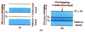
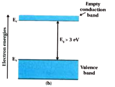
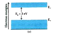
  3. Explain conductor (metal), insulator and semiconductor by drawing diag...

    Text Solution

    |

  4. Explain the crystalline structure by writing the electronic configurat...

    Text Solution

    |

  5. Explain the concept of the hole in the semiconductor.

    Text Solution

    |

  6. Explain with diagram, how current flows due to electron and hole in pu...

    Text Solution

    |

  7. Explain the change in the band with the temperature of the intrinsic ...

    Text Solution

    |

  8. Why is it required to add impurity in pure semiconductor? Mention it's...

    Text Solution

    |

  9. What is n-type semiconductor? Name the majority and minority carriers ...

    Text Solution

    |

  10. What is p-type semiconductor? Name the majority and minority carriers ...

    Text Solution

    |

  11. Explain n and p-type semiconductor based on band theory.

    Text Solution

    |

  12. Explain recombination coefficient of intrinsic semiconductor and obtai...

    Text Solution

    |

  13. Write four points in distinguishing between p-type semiconductor and n...

    Text Solution

    |

  14. Write the difference between intrinsic and extrinsic semiconductor.

    Text Solution

    |

  15. Which is the primary constitutional unit for diode and transistor?

    Text Solution

    |

  16. How p-n junction diode is formed ? And explain depletion layer and bar...

    Text Solution

    |

  17. What is depletion barrier?

    Text Solution

    |

  18. Write short on semiconductor diode.

    Text Solution

    |

  19. State the methods of connection of p-n junction.

    Text Solution

    |

  20. What is forward bias and reverse bias ?

    Text Solution

    |