Home
Class 12
PHYSICS
When is the p-n junction called reverse ...

When is the p-n junction called reverse bias and explain the change in p-n junction from this type of connection.

Text Solution

Verified by Experts

When and external voltage (V) is applied across the diode such that n-side is positive and p-side is negative it is said to be reverse biased. This is shown in figure.

Diagram (b) for the circuit is as follows :

The applied voltage mostly drops across the depletion region according to figure (a).
The direction of applied voltage `V_(0)` is same as the direction of barrier potential V. As a result, the barrier height increases and the depletion region widens due to the change in the electric field.

The effective barrier height under reverse bias is `V+V_(0)`.
In figure (c ), the battery is not connected to p-n junction, potential barrier `V_(0)` is shown as 1 and when voltage of the external battery is applied, its effective potential barrier `V_(0)+V` is shown as 2.
This suppresses the flow of electrons from `n to p` and holes from `p to n` due to effective depletion barrier potential means current are disputed due to majority charge carriers hence diffusion current is not obtained.
Although some minority charge carriers pass through the junction due to the high voltage applied by external battery hole in n-region and electron in p-region and current flow in reverse direction is called reverse current. However, for large reverse voltage, the increase in reverse current shows less.
Reverse current does nto depend only on the applied voltage. The current is not limited by the magnitude of the applied voltage but is limited due to the concentration of the minority carrier on either side of junction.
Some voltage is also sufficient to across the junction for minority carriers.
The reverse bias voltage varies from about 10 V to 15 V.
Here current obtained in the order of microampere `(muA)`.
Promotional Banner

Topper's Solved these Questions

  • SEMICONDUCTOR ELECTRONICS : MATERIALS, DEVICES AND SIMPLE CIRCUITS

    KUMAR PRAKASHAN|Exercise Section-B : Numericals (Numerical From Textual illustrations)|16 Videos
  • SEMICONDUCTOR ELECTRONICS : MATERIALS, DEVICES AND SIMPLE CIRCUITS

    KUMAR PRAKASHAN|Exercise Section-B : Numericals (Numerical From Textual Exercise)|15 Videos
  • SEMICONDUCTOR ELECTRONICS : MATERIALS, DEVICES AND SIMPLE CIRCUITS

    KUMAR PRAKASHAN|Exercise Section-D : Multiple Choice Questions (MCQs) (MCQs asked in Competitive Exams)|129 Videos
  • SAMPLE QUESTION PAPER

    KUMAR PRAKASHAN|Exercise PART-B SECTION-C|5 Videos
  • WAVE OPTICS

    KUMAR PRAKASHAN|Exercise SECTION-D (MULTIPLCE CHOICE QUESTIONS (MCQS)) (MCQS FROM DARPAN BASED ON TEXTBOOK)|239 Videos

Similar Questions

Explore conceptually related problems

The p-n junction is a :-

p-n junction is called as forward biased when

In given diagram which p-n junction in reverse biased

When p-n junction diode is forward biased ………

The depletion region of a p-n junction contains :-

Increasing reverse bias voltage applied to p-n junction diode ……..

When a forward bias is applied to a p-n junction, it

Reverse bias applied to a junction diode ……

The depletion layer in the p-n junction region is caused by ……

KUMAR PRAKASHAN-SEMICONDUCTOR ELECTRONICS : MATERIALS, DEVICES AND SIMPLE CIRCUITS -Section-A : Questions - Answers
  1. State the methods of connection of p-n junction.

    Text Solution

    |

  2. What is forward bias and reverse bias ?

    Text Solution

    |

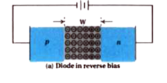
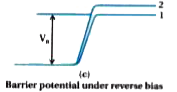
  3. When is the p-n junction called reverse bias and explain the change in...

    Text Solution

    |

  4. What is static characteristic of p-n junction and write its types.

    Text Solution

    |

  5. Explain the forward characteristics of the p-n junction diode by drawi...

    Text Solution

    |

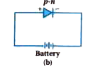
  6. Explain the reverse characteristics of p-n junction diode by circuit d...

    Text Solution

    |

  7. What is rectification and rectifier ? Why p-n junction diode is used a...

    Text Solution

    |

  8. Write the principle of rectifier.

    Text Solution

    |

  9. Explain the use of the junction diode as a half wave rectifier by draw...

    Text Solution

    |

  10. Explain the use of junction diode as a full wave rectifier by drawing ...

    Text Solution

    |

  11. Describe the simple filter circuit for obtaining smooth rectified volt...

    Text Solution

    |

  12. Write short note on zener diode.

    Text Solution

    |

  13. Explain the use of Zener diode as a voltage regulator.

    Text Solution

    |

  14. What are optoelectronic devices? Give the names of such major devices.

    Text Solution

    |

  15. Explain construction and working of photodiode.

    Text Solution

    |

  16. Explain the design, working, uses and benefits of light emitting diode...

    Text Solution

    |

  17. Describe construction, working and use of the solar cell.

    Text Solution

    |

  18. What are the ideal materials for fabrication of solar cell? and give t...

    Text Solution

    |

  19. What is digital signal ? What mathematical method are expressed in it?

    Text Solution

    |

  20. write types of logic system.

    Text Solution

    |