A
B
C
D
Text Solution
Verified by Experts
The correct Answer is:


Topper's Solved these Questions
SEMICONDUCTOR ELECTRONICS : MATERIALS, DEVICES AND SIMPLE CIRCUITS
KUMAR PRAKASHAN|Exercise Section-D : Multiple Choice Questions (MCQs) (MCQs From .DARPAN. Based On Textbook)|116 VideosSAMPLE QUESTION PAPER
KUMAR PRAKASHAN|Exercise PART-B SECTION-C|5 VideosWAVE OPTICS
KUMAR PRAKASHAN|Exercise SECTION-D (MULTIPLCE CHOICE QUESTIONS (MCQS)) (MCQS FROM DARPAN BASED ON TEXTBOOK)|239 Videos
Similar Questions
Explore conceptually related problems
KUMAR PRAKASHAN-SEMICONDUCTOR ELECTRONICS : MATERIALS, DEVICES AND SIMPLE CIRCUITS -Section-D : Multiple Choice Questions (MCQs) (MCQs asked in Competitive Exams)
- Name the gate, which represent the Boolean expression y=bar(A*B)
Text Solution
|
- An electron hole pari is formed when light of maximum wavelength 6000...
Text Solution
|
- The boolean expression of NOR gate is…….
Text Solution
|
- Which of the following is not a type of tissue ?
Text Solution
|
- The output of AND gate is 1, so ……
Text Solution
|
- The ratio of resistance of forward bias and reverse bias in p-n connec...
Text Solution
|
- A sinusoidal voltage of peak value 220 volts is connected to a diode ...
Text Solution
|
- In a zener diode, the reverse bias voltage is 3V and width of the depl...
Text Solution
|
- Gate can be obtained by shorting both the input terminals of a NOR gat...
Text Solution
|
- The figure shows the input signal A, input signal B and output signal ...
Text Solution
|
- What kind of p-n junction diode does not require any kind of bias?
Text Solution
|
- Which logic gate is represented by the following logic gates?
Text Solution
|
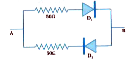
- For the circuit shown in the figure, calculate the equivalent resistan...
Text Solution
|
- The value of beta of a transistor is 19. The value of alpha will be ……
Text Solution
|
- The wavelength of photon having energy of 35 keV is …….. (h=6.625xx1...
Text Solution
|
- The band gaps of a conductor, semiconductor and insulator are respecti...
Text Solution
|
- Which of following gates produces output of 1 ?
Text Solution
|
- The electric field for p-n junction is 1xx10^(6) V/m and depletion reg...
Text Solution
|
- In p-n junction the width of space charge region is approximately ….. ...
Text Solution
|
- ……as a impurity, when added in Si or Ge P- type semiconductor is obtai...
Text Solution
|