Home
Class 12
PHYSICS
Draw the tramsfer characteristic curve o...

Draw the tramsfer characteristic curve of a base biased transistor in CE configuration. Explain clearly how the active region of the `V_o" versus " V_i` curve in a transistor is used as an amplifier.

Text Solution

Verified by Experts

(a)
In the active region, a (samll) increase of Vi results in a (large, almost linear) increase in `I_c`. This results in an increase in the voltage drop across `R_c`.
(b) When `V_i` becomes greater than 0.6 V, the transistor is an active state with some current. `I_c` in the output path. The transistor is operated as a switch. As long as `V_i` is low and unable to forward-bias the transistor, `V_0" is high. If "V_i` is high enough to derive the transistor into saturation, the `V_0` is low, very near to zero.
When the transistor is not conducting, it is said to be switched off and when it is driven into saturation,
Promotional Banner

Topper's Solved these Questions

  • XII BOARDS

    XII BOARD PREVIOUS YEAR PAPER ENGLISH|Exercise SET-II, DELHI BOARD|4 Videos
  • XII BOARDS

    XII BOARD PREVIOUS YEAR PAPER ENGLISH|Exercise SET-III, DELHI BOARD|4 Videos
  • XII BOARDS

    XII BOARD PREVIOUS YEAR PAPER ENGLISH|Exercise SET -III|4 Videos
  • SAMPLE PAPER 2019

    XII BOARD PREVIOUS YEAR PAPER ENGLISH|Exercise SECTION D|6 Videos

Similar Questions

Explore conceptually related problems

The transfer characteristics of a base biased transistor has the operation regions, namely, cutoff, active region and saturation region. For using the transistor as an amplifier it has to operate in the

Fig.shows that transfer characteristics of a base biased CE transistor. Which of the following statements are true?

Fig.shows that transfer characteristics of a base biased CE transistor. Which of the following statements are true?

Transfer characterstics [output voltage (V_(o)) vs. input voltage (V_(i)) ] for a base biased transistor in CE configuration is as shown in the figure. For using transfor as a which, it is used

Draw a labelled circuit diagram of n - p - n germanium transistor in common emitter configuration. Explain briefly, how this transistor is used as a voltage amplifier.

Draw typical output characteristics of an n-p-n transistor in CE configuration. Show how these characteristics can be used to determine output resistance.

Draw the labelled circuit diagram of a common-emitter transistor amplifier : Explain clearly how the input and output signals are in opposite phase.

Draw the diagram of the circuit arangement used for studying the 'input' and the 'output' characteristics of an n-p-n transistor inits CE configuration. Briefly explain how these two types of characteristics are obtained and draw these characteristics. (b) 'Define' the terms (i) Input resistance, (ii) Output resistance , (iii) Current amplification factor, for a given transistor.

(a) Draw the circuit arrangement for studying the input and output characteristics of an n-p-n transistor in CE configuration . With the help of these characteristics define (i) input resistance , (ii) current amplification factor . (b) Describe briefly with the help of a circuit diagram how an n-p-n transistor is used to produce self-sustained oscillations .

(i) Figure shows the input waveform which is converted by a device .X. into an output wavefrom. Mane the device and explain its working using the proper circuit. (ii) Draw the forward bias and reverse blas circuit for the basic component of the device and draw the characterstics. Explain clearly which region of the curve is used in an amplifier.

XII BOARD PREVIOUS YEAR PAPER ENGLISH-XII BOARDS-PHYSICS (Theory) [SET -I]
  1. Define the term 'wattles current'.

    Text Solution

    |

  2. When monochromatic light travels from one medium to another, its wavel...

    Text Solution

    |

  3. In the youngs double slit experiment ,the slit sepration is 1mm ,the d...

    Text Solution

    |

  4. A magnetic needle free to rotate in a vertical plane parallel to magne...

    Text Solution

    |

  5. Two convex lenses of same focal length but of aperture A(1) and A(2)(A...

    Text Solution

    |

  6. Name the semiconductor device that can be used to regulate an irregula...

    Text Solution

    |

  7. How are infrared waves produced? Why are these referred to as 'heat wa...

    Text Solution

    |

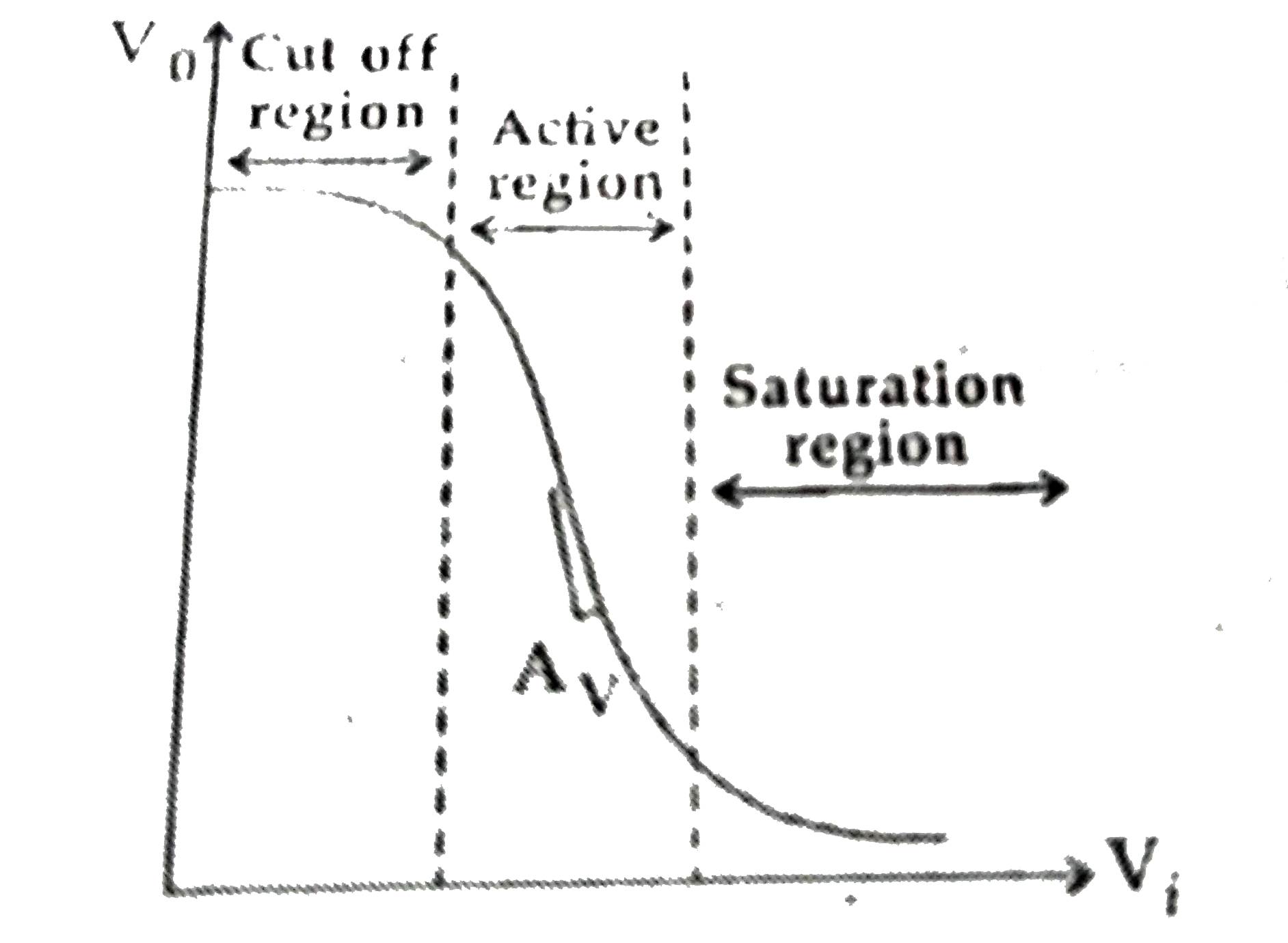
  8. Draw the tramsfer characteristic curve of a base biased transistor in ...

    Text Solution

    |

  9. Define modulation index. Why is it generally kept less than one ?

    Text Solution

    |

  10. A conductor of length L is connected to a dc source of emf epsilon. If...

    Text Solution

    |

  11. Using Gauss's law obtain the expression for the electric field due to ...

    Text Solution

    |

  12. An electron and a photon each have a wavelength 1.00 nm. Find (i) ...

    Text Solution

    |

  13. Draw a schematic diagram showing the (i) ground wave (ii) sky wave and...

    Text Solution

    |

  14. Describe Young's double slit experiment to produce interference patter...

    Text Solution

    |

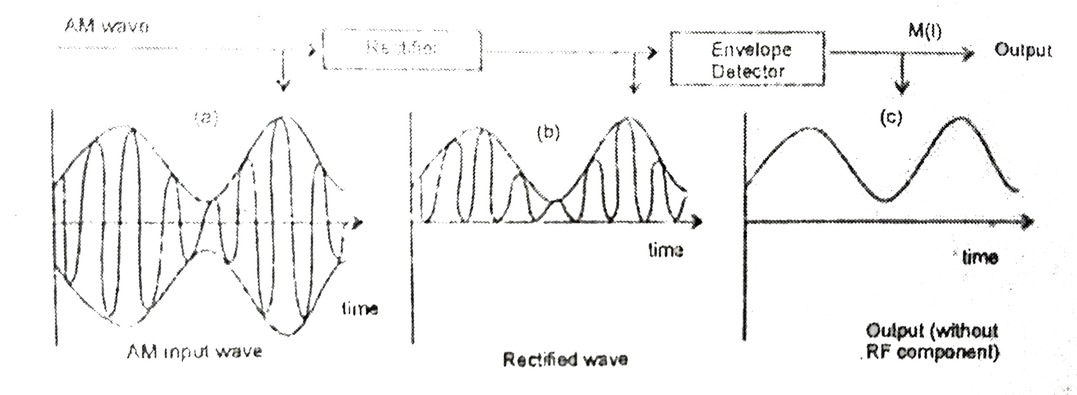
  15. (a) Describe briefly, with the help of suitable diagram, how the tran...

    Text Solution

    |

  16. State the law of radioactive decay. Plot a graph showing the number (N...

    Text Solution

    |

  17. State Biot-Savart law, giving the mathematical expression for it. Us...

    Text Solution

    |

  18. (a) Draw a ray diagram to show regraction of a ray of monochromatic l...

    Text Solution

    |

  19. (a) Obtain lens makers formula using the expression n2/v-n1/u=((n2-...

    Text Solution

    |

  20. (i) with the help of a labelled diagram, describe briefly the underly...

    Text Solution

    |